 |
| schemtic digram circuit of Stereo Audio Power Amplifier 11 Watt using LM4752 |
External link:
LM4752 Stereo Audio Power Amplifier 11 Watt Datasheet – www.national.com
author: Wiring Diagram
e-mail:
web site: http://www.wiringdiagrams21.com/
D.I.Y, Free Electronic Circuits, Hobby Circuits, Audio-video circuits, Radio circuits, Power supply, Digital Circuits, Embedded Circuits, Amplifiers, Power Amplifier, Data Sheet, Service Manual, Free Download.


 |
| schemtic digram circuit of Stereo Audio Power Amplifier 11 Watt using LM4752 |
Posted by abe 0 comments
Labels: LM4752, Power Amplifier, Schematics | View blog reactions
|
Bookmark this post:
|
|
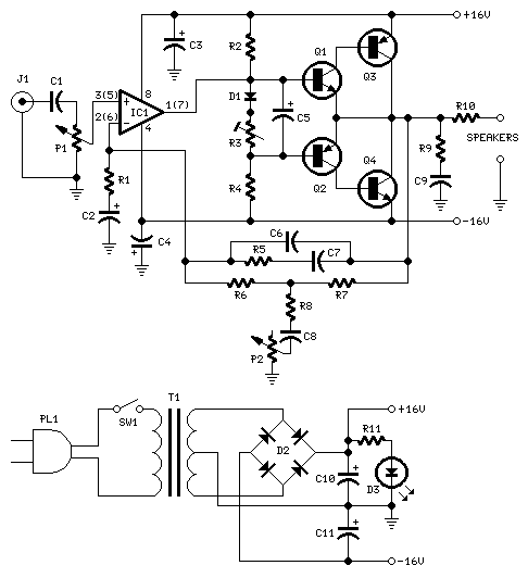
Parts:
P1 22K Log.Potentiometer (Dual-gang for stereo)
P2 100K Log.Potentiometer (Dual-gang for stereo)
R1 820R 1/4W Resistor
R2,R4,R8 4K7 1/4W Resistors
R3 500R 1/2W Trimmer Cermet
R5 82K 1/4W Resistor
R6,R7 47K 1/4W Resistors
R9 10R 1/2W Resistor
R10 R22 4W Resistor (wirewound)
C1,C8 470nF 63V Polyester Capacitor
C2,C5 100uF 25V Electrolytic Capacitors
C3,C4 470uF 25V Electrolytic Capacitors
C6 47pF 63V Ceramic or Polystyrene Capacitor
C7 10nF 63V Polyester Capacitor
C9 100nF 63V Polyester Capacitor
D1 1N4148 75V 150mA Diode
IC1 NE5532 Low noise Dual Op-amp
Q1 BC547B 45V 100mA NPN Transistor
Q2 BC557B 45V 100mA PNP Transistor
Q3 TIP42A 60V 6A PNP Transistor
Q4 TIP41A 60V 6A NPN Transistor
J1 RCA audio input socket
Power supply parts:
R11 1K5 1/4W Resistor
C10,C11 4700uF 25V Electrolytic Capacitors
D2 100V 4A Diode bridge
D3 5mm. Red LED
T1 220V Primary, 12 + 12V Secondary 24-30VA Mains transformer
PL1 Male Mains plug
SW1 SPST Mains switch
schematic/circuit diagram
 |
| schematic diagram circuit of 10 Watt Audio Power Amplifier with Bass-boost |
Posted by abe 0 comments
Labels: NE5532, OPA2134, Power Amplifier, Schematics, TL072, TLE2141C | View blog reactions
|
Bookmark this post:
|
|
The creator of THIS PAGE or the ISP(s) hosting any content on this site take NO responsibility for the way you use the information provided on this site. These circuits here are for educational purposes only and SHOULD BE VIEWED ONLY. If you download any files to view them, you are agreeing to delete them within a 24 hour period. If you are affiliated with any government, or ANTI-Piracy group or any other related group or were formally a worker of one you CANNOT enter this web site, cannot access any of its files and you cannot view any of the HTML files. All the objects on this site are PRIVATE property and are meant for previewing only. If you enter this site without following these agreements you are not agreeing to these terms and you are violating code 431.322.12 of the Internet Privacy Act signed by Bill Clinton in 1995 and that means that you CANNOT threaten our ISP(s) or any person(s) or company storing these files, cannot prosecute any person(s) affiliated with this page which includes family, friends or individuals who run or enter this web site. IF YOU DO NOT AGREE TO THESE TERMS THEN LEAVE.
All files are found using legitimate search engine techniques. This site does not and will not condone hacking into sites to create the links it list. We will and do assume that all links found on the search engines we use are obtained in a legal manner and the webmasters are aware of the links listed on the search engines. If you find a URL that belongs to you, and you did not realize that it was "open to the public", please use the report button to notify the blogmaster of your request to remove it. This is not an invitation for webblog haters to spam with requests to remove content they feel that is objectionable and or unacceptable. Proof of URL ownership is required.
NOTICE: This Blog Has Already Been Reviewed And Accepted By Blogger.com


My blog is worth $564.54.
How much is your blog worth?


 I love using "Real Link Finder"! It lets me find on-topic blogs where I can leave my own comments and a "Real" link back to my website! Get your own copy of this free blog commenting software by clicking here!