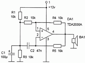
This chip amplifier NCH TDA2030A company ST Microelectronics enjoys well-deserved popularity among radio amateurs. It has a high electrical performance and low cost, which allows for the least cost to collect her high UNCH capacity of up to 18 Watts. But not everyone is aware of its hidden virtues: it turns out at the IMS can collect a number of other useful devices. TDA2030A chip is a 18 W Hi-Fi class AB power amplifier or a driver for UNCH capacity of up to 35 W (with strong external transistor) . It provides high output current, has a small harmonic and intermodulation distortion, wide bandwidth reinforced signal, a very low level of own noise, built protection against short circuits output, an automatic system for limiting the power dissipation, holding a working point of output transistors IMS in a safe area. This chip implemented in the shell Pentawatt and has a 5 findings. At first, a brief look at several standard charts IMS application - bass amplifiers. The model scheme to include TDA2030A shown in Figure 1.

This chip is included on the scheme neinvertiruyuschego amplifier. Gain is determined by the ratio of resistance resistors R2 and R3, forming a chain of OOS. It is calculated by the formula Gv = 1 + R3/R2 and can be easily changed by selecting the resistance of a resistor. Usually this is done through the resistor R2. As can be seen from the formula, reducing resistance of the resistance increasing the gain (sensitivity) UNCH. Capacity capacitor C2 light of the fact that its capacitance Hs = 1 / 2? FS at a lower operating frequency was lower than R2 for at least 5 times. In this case, at a frequency of 40 Hz Hs 2 = 1 / 6, 28 * 40 * 47 * 10 -6 = 85 ohms. Input resistance is determined by the resistors R1. As VD1, VD2 can use any silicon diodes with a current I OL 0.5 ... 1 A and U OBR more than 100, for example KD209, KD226, 1N4007. Hook-IMS in the case of a unipolar power source is illustrated in Figure 2.

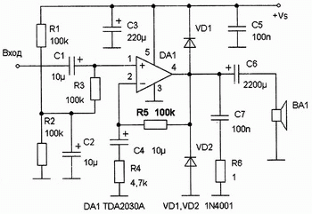
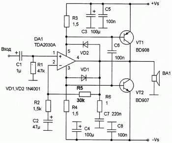
Divisor R1R2 and resistor R3 form a chain of shifting to get at the outlet of IMS (conclusion 4) voltage equal to half the supply. This is necessary to strengthen both symmetrical poluvoln input. The parameters of this scheme at Vs = +36 V correspond to the scheme shown in Figure 1, when the power source of ± 18 V. Example of chips as a driver for UNCH with powerful external transistor is shown on Fig.3.

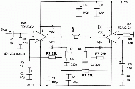
When Vs = ± 18 V at 4 ohm load amplifier power 35 Watts. In the food chain IMS includes resistors R3 and R4, a drop which is opening for transistors VT1 and VT2, respectively. In a small output (input voltage) current consumed IMS, low and the voltage drop on resistor R3 and R4 not enough to open the transistors VT1 and VT2. As the input voltage increases output and consumption current of IMS. In pursuing its value 0.3 ... 0.4 A voltage drop on resistor R3 and R4 will be 0.45 ... 0.6 V. begin to open transistors VT1 and VT2, while they will be included alongside the internal transistors IMS. As VT1 and VT2 can use any pair of complementary transistors respective capacities, for example KT818, KT819. Square scheme incorporating IMS is illustrated in Figure 4.

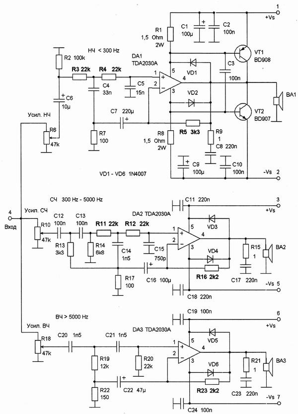
The signal from a commercial IMS DA1 via divider R6R8 at inverting input DA2, which provides chips in the opposite. At the same time increasing the voltage at the load and, consequently, increased power output. When Vs = ± 16 V at 4 ohm load power output reaches 32 Watts. For fans of the two-, three-UNCH this IMS - an ideal solution, because it can directly collect active LPF and HPF. The scheme of three-UNCH shown on Fig.5.

Low channel (NCH) is made on the scheme with powerful output transistors. At the entrance IMS DA1 included LPF R3C4, R4C5, the first link LPF R3C4 included in the chain of OOS amplifier. Such designs allows simple control (without increasing the number of links) get high enough slope recession ACHH filter. Medium (SCH) and high-frequency (HF) channel amplifier assembled on a model scheme for IMS DA2 and DA3 respectively. At the entrance SCH channel includes FHP C12R13, C13R14 and LPF R11C14, R12C15, which together provide the bandwidth of 300 ... 5000 Hz. The filter frequency channel assembled in the cell C20R19, C21R20. The cutoff frequency of each link, or LPF HPF can be calculated by the formula f = 160/RC, where the frequency f expressed in Hz, R - in kiloohm, S - in mikrofarad. These examples do not exhaust the possible application of IMC TDA2030A as a bass amplifier. For example, instead of feeding dvuhpolyarnogo Products (Fig.3, 4), you can use a unipolar power. To do this, minus the power source should zazemlit at neinvertiruyuschy (output 1) input file offset, as shown in Figure 2 (elements R1-R3 and S2). Finally, the output IMS between 4 and load the conclusion should include electrolytic capacitor, a blokirovochnye capacitors on the chain-Vs from the scheme should be deleted.
TDA2030A IMS represents nothing more than an operational amplifier with a powerful weekend cascade and a very good performance. Based on this, have been designed and tested with several non-standard inclusion. Some schemes has been tested "live" on the breadboard, some - modeled in the Electronic Workbench.
Powerful repeater signal.

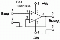
The signal at the output device Fig.6 repeats in shape and amplitude of the input, but has great power, that is scheme can work at low pressures. Repeater can be used, for example, umoschneniya power supplies, increasing the output of low-frequency generator (so you can immediately feel the head speaker or acoustic systems). The band working frequency repeater is linear from dc to 0.5 ... 1 MHz, more than enough for the generator NCH.
Umoschnenie power sources.


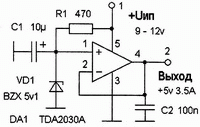
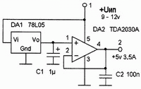
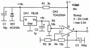
This chip is included as a repeater signal, output voltage (output 4) is the input (output 1), and the output current can reach values of 3.5 A. Thanks to the built-protection scheme is not afraid of short circuits in the load. The stability of output voltage stability is determined by reference, that is stabilitrona VD1 Fig.7 and integral stabilizer DA1 Fig.8. Naturally, the pattern shown in Fig.7 and Fig.8, you can collect stabilizers and other stress, just need to keep in mind that the total (full) power dissipated by the chip should not exceed 20 Watts. For example, you need to build a stabilizer at 12 V and current 3 A. There is a ready source of food (transformer, rectifier and filter capacitor), which gives U IP = 22 V, with the necessary current load. Then on the chip occurs voltage drop U IMS IP = U - U VYH = 22 -12 V = 10V and a current load 3 A dissipated power reaches values of R = U RAS IMS * I * N = 10B = 3A W 30, that exceeds the maximum value for TDA2030A. The maximum permissible voltage drop in the IMS can be calculated using the formula:
U IMS = R RAS.MAH / I N. In our example, U IMS = 20 W / 3 A = 6.6 V, thus the maximum voltage rectifier must be U = U new IP + U IMS = 12V + 6.6 V = 18.6 B. The number of turns of the transformer secondary windings will diminish. Resistance ballast resistor R1 in the pattern shown in Fig.7, you can count on the formula:
R1 = (U IP - U CT) / I ST, where U ST and ST I - respectively voltage and current stabilization stabilitrona. The limits of the current stabilization can be found in the handbook, in practice for low stabilitronov his choosing within 7 ... 15 mA (typically 10 mA). If the current in the above formula to express in milliampere, the amount of resistance to get in kiloomah.
A simple laboratory power supply.

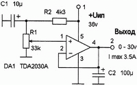
By varying the voltage at the entrance of IMS using potentiometer R1, produced a smooth adjustable output voltage. The maximum current, given a chip, depending on the output voltage and restricted the same maximum dissipated power at IMS. Calculate it could be the formula:
I MAX = R RAS.MAH / U IMS
For example, if the output voltage U billed VYH = 6, the chip is happening voltage drop U IMS IP = U - U VYH = 36 - 6 = 30, therefore, the maximum current is I MAX = 20 W / 30 = 0.66 A. When U VYH = 30 V maximum current can reach a maximum of 3.5 A, as well as a drop in the IMS slightly (6).
Stabilized laboratory power supply.

Source stabilized reference voltage - chip DA1 - powered by Parametric stabilizer at 15, collected at stabilitrone VD1 and resistor R1. Should IMS nurture DA1 directly from the source +36 V, it can be easily damaged (the maximum input voltage for IMS 7805 is 35 V). IMS DA2 included on the scheme neinvertiruyuschego amplifier gain which is defined as 1 + R4/R2 and is 6. Consequently, the output voltage adjustment potentiometer R3 can take the value from nearly zero to 5 * 6 = 30 V. With regard to the maximum output current, for this scheme true all this for a simple laboratory power supply (Fig.9). If it is less regulated output voltage (for example, from 0 to 20 in the U IP = 24), elements VD1, S1 can be excluded from the scheme, but instead R1 set the jumper. If necessary, the maximum output voltage can change the selection of resistance resistor R2 and R4.
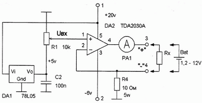
An adjustable current source.

At the entrance inverting IMS DA2 (concludes 2), thanks to the OOS through resistance load, supported by tension U BX. As can be seen from the formula, load current does not depend on the resistance loads (of course, up to certain limits, due to end-voltage IMS). Therefore, changing the U BX from zero to 5 V using potentiometer R1, with the fixed value of resistance R4 = 10 ohms, can be controlled through the current strain of 0 ... 0.5 A. The device can be used for charging batteries and electroplating elements. Charging current stable throughout the cycle of charging and does not depend on the amount of discharge of the battery or the instability of the supply network. The maximum charging current, displayed using potentiometer R1, you can change, increasing or decreasing resistance resistor R4. For example, when R4 = 20 ohms, it has a value of 250 mA, and with R4 = 2 ohms reaches 2.5 A (see formula above). For the scheme are fair restrictions on the maximum output current, both for stabilizing voltage circuits. Another application of a powerful inhibitor of current - measuring small resistance through voltmetra on a linear scale. Indeed, if the value of a current exhibit, for example, 1 A, is connected to the scheme resistor 3 ohms resistance, Ohm's law to get the voltage drop its U = l * R = l A * 3 ohms = 3 V, and connecting, say, resistor resistance 7.5 ohms, we get a drop 7.5 V. Of course, this current can be measured only powerful Low resistors (3 V at 1 A - is 3 W, 7.5 V * 1 A = 7.5 W) But you can reduce the measured current and use the voltmeter to the lower limit of measurement.
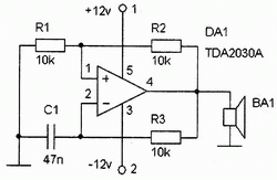
A powerful generator of rectangular pulses.


Plans powerful generator of rectangular pulses are shown in Fig.12 (with bipolar diet) and Fig.13 (with unipolar meals). Plans can be used, for example, the device alarm. This chip includes a Schmitt trigger, and the whole scheme is a classic relaxation RC-oscillator. Consider the job figures. 12. Let's assume that at the time of the power output of IMS is moving towards a positive level of saturation (U VYH = + U IP). Capacitor C1 begins to be charged through resistor R3 with a constant time-Cl R3. When the voltage on C1 will reach half a positive voltage power source (+ U IP / 2), IMS DA1 switch to a negative saturation (U VYH =-U IP). Capacitor C1 will discharged through resistor R3 at the same time Cl R3 to the voltage (-U IP / 2) when the IMS again switches into a positive state of saturation. The cycle will be repeated with a 2,2 C1R3, regardless of the power supply voltages. Frequency pulses can count on the formula:
f = l / 2,2 * R3Cl. If the resistance to express kiloomah and capacity in mikrofaradah, the frequency will get in kilohertz.
A powerful low-frequency generator harmonic oscillations.

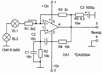
An electric circuit powerful low-frequency generator harmonic oscillations is shown in Fig.14. The generator gathered on a bridge Wines, formed by elements of DA1 and S1, R2, C2, R4, providing the necessary phase shift in the chain of PIC. Gain voltage IMS, with the same values of Cl, C2 and R2, R4 should be exactly equal to 3. With less importance Ku fluctuations fade, and an increased - dramatically increasing distortion of the output signal. Gain voltage determined resistance filament bulbs ELI, EL2 and resistors Rl, R3 and is Ky = R3 / Rl + R EL1, 2. Lamps ELI, EL2 serve as elements with variable resistance in the chain of OOS. When increasing the output voltage resistance of the filament lamp by heating increases, causing a decrease gain DA1. Thus, stabilizing the amplitude of the output signal generator, and minimize distortions of form sinusoidalnogo signal. Minimum distortion at the maximum possible output amplitude sought through podstroechnogo resistor R1. To exclude the impact of stress on the frequency and amplitude of the output signal at the output of the generator includes a chain R5C3, frequency oscillations generated can be determined by the formula:
f = 1/2piRC. Generator can be used, for example, in the repair and inspection heads speaker or speakers.
In conclusion, the chips must be installed on the radiator with ohlazhdaemoy surface area of not less than 200 cm 2. When razvodke agents of the printed circuit board for the amplifier must be Bass track to "earth" tires for input, as well as the power source and output summed with the different parties (conductors to these terminals should not be a continuation of one another, and assembled together to form stars "). This is necessary to minimize the background of the AC and eliminate possible self-amplifier with output power close to the maximum.
By the magazine Радіоаматор
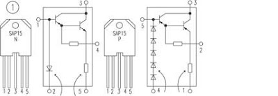 SAP15N / P structure see Figure 1.