source: http://cappels.org/dproj/edfet/edfet.html
The EDFET drives like a FET, but with the bias stability of bipolar. Amps of output current can be controlled by milliamps of input current. The current gain is a design choice dictated by bandwidth. Two of things you have to consider when adding a power output stage to an op-amp circuit are the frequency response and the cross-over distortion in that stage.
This is especially true with wide band amplifiers, where the unity gain crossover needs to be at several hundred kilohertz. The stage is driven much the same as a complimentary pair output stage, but with the current gain that comes with using FETs., and with feedback within the output stage that that extends the buffer's bandwidth and regulates the quiescent current. More predictable operation allows the designer to design a circuit lower overall power dissipation and better closed loop stability.
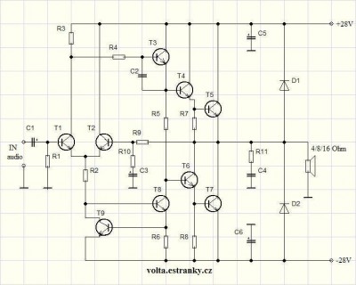
The EDFET complimentary buffer is made up of a pair of unity gain buffers, one that drives in the positive direction and the other that drives in the negative direction. Pictured above is the positive driving half of the output stage.
Gain to make the output signal track the input signal comes from inverting transistor, Q1. The input signal is applied to the emitter of Q1 and the output of the amplifier is raised one diode drop to match the forward base-emitter drop of Q1, by diode connected transistor Q2. The buffer's offset is determined by the log of the magnitude of the mismatch in the emitter currents in Q1 and Q2, and it is directly proportional to the absolute temperature.
Since the saturation current usually isn't published for the transistors this expression is only usefully for appreciating the dependence of junction voltage on current and temperature. You can come up with your own value of I0 for a given transistor if you know all the other parameters and solve the above formula for I0. By the way, since, for most practical uses, you will be running at more than a thousand times the saturation current, the "+1" term can be dropped from practical calculations.
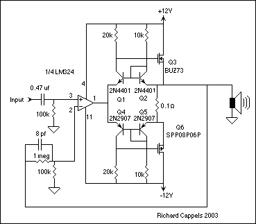
As an example, for the audio amplifier using a EDFET buffer shown in Figure 1. The following assumptions are applied: The maximum output voltage is 5 VDC with respect to ground, the power supply (VA) is 12 VDC, the maximum gate voltage is 8 VDC, the input capacitance, Ciss of the BUZ73 is 500 pf, and an...
http://cappels.org/dproj/edfet/edfet.html
Discrete Buffer: Diamond Buffer
Discrete Buffer: JISBOS Buffer
