1. Power Amplifier Basic Circuit Characteristics
Complementary symmetric OTL amplifier basic circuit as shown in Figure 1. Where: C1 for the signal input coupling element, should be noted that the actual circuit in the polarity should be consistent with the potential situation. R1 and R2 bias circuit composed of BG1, BG1 to provide a static operating point, but also in the entire circuit to play the role of DC negative feedback. Asked to approve R1 is greater than the current BG1 base current of at least five times, according to β is 100, Ic1 for 2mA calculation, R1 should be no more than 6k, it is given as a 5.1k; C1 accordingly, to set at 22μ, it is 20Hz signal on the impedance of 362Ω; R2 must be in accordance with the specific voltage of the power to determine, or about R1 (E/2-0.6) / 0.6, in accordance with 32V voltage value should be taken as about 120K, the exact value of the actual debugging by making BG1 collector voltage of 15.4V to get.

C2 and R3 constitute a bootstrap circuit, require R3C2> 1 / 10, (R3 + R4) Ic1 = E/2-1.2, due to the exchange of R4 is the BG1 load resistance, as far as possible to take bigger, R3 normally taken within the 1k. In accordance with 32V supply voltage value and Ic1 to 2mA calculations, R3 and R4 of and for the 7.2k, the actual will of R3 to 820Ω, R4 to the 6.8k, Ic1 compared to 1.94mA; C2 is therefore desirable to 220μ.
R5 and D are BG2, BG3 complementary bias control circuit components, to BG2, BG3 together provide a suitable quiescent point, to eliminate crossover distortion as much as take a small value, according to the experimental results are generally obtained in the 3mA ~ 4mA; R5 Resistance to change can BG2 and BG3 base voltage drop between the changes in the work to achieve the adjustment of its static, and R5 in series D is to compensate for BG2, BG3 launch junction threshold voltage changes with temperature, preferably in two only the series diode junction fired up and compensate for the threshold voltage of complementary tube changes with temperature, so that complementary management quiescent operating point stability. Omitted to simplify the use of a diode circuit. In parallel with BG2, BG3 base between the C4, can reduce the dynamic work of the ΔUAB, generally taken to be 47μ; C3 is to prevent the BG1 the exchange of high-frequency self-excited negative feedback capacitor, generally taken to be 47P ~ 200P.
BG1 from voltage amplification role in this circuit is known as the incentive level, require Buceo> E, Iceo ≤ Ic1/400 = 5μA, β = 100 ~ 200, so it should use low-power low-noise transistor. BG2 and BG3 are complementary current amplification pole, respectively, and BG4, BG5 constitute a composite tube to amplify the output current require Buceo> E, Iceo ≤ Ic2/100 = 30μA, β = 100 ~ 200. In the BG4, BG5 using ordinary high-power tubes instead of three has been made within the composite pipe under high-power 3, BG2 and BG3 need to provide the post-class high-power three tubes of more than 100mA peak drive current, it should the use of power three tubes. BG4 and BG5 is responsible for the amplification of high-power output current control, quiescent current is desirable in the 10mA ~ 30mA, asked Buceo> E, Iceo ≤ Ic4/100 = 0.1mA, β = 50 ~ 100. BG4 and BG5 the maximum limit of current Imax should be greater than the largest amplitude of the output current times the big one, can ensure the maximum amplitude of the output current when β> 10.
R6 and R7 are BG4 and BG5 quiescent operating point adjustment of shunt resistor, the dynamic work of the streaming effect can be negligible. The Ube4 and Ube5 are equal to 0.6V standard parameters, by the complementary current amplification level obtained in the static working current of 3mA ~ 4mA, calculate the R6 and R7 should be taken as 220Ω. In fact, the power may be a difference of three tubes Ube larger, BG4 and BG5 of Ube be carried out by matching the measured use of the bootstrap circuit to work with half the total current magnification composite pipe shall be constructed without the aid of the work of the bootstrap circuit The other half of the composite pipe is smaller.
R8 and R9 are to prevent the BG4 and BG overcurrent limiting resistor, generally take between the 0.2Ω ~ 0.5Ω. Will use the 200mm long, diameter φ0.08 both ends of the enameled wire were welded over the 1k resistor at both ends to fold up enameled wire can be wrapped around the resistor. Is equivalent to the role of fuse fuse belongs to the simplest non-smart Limit blown protection methods.
C5 and C6 is the signal output capacitor, with a small capacitor in parallel with the large capacitor up and use, it can eliminate large-capacity capacitor has a larger internal inductance for high-frequency signals obstacles. Note that it is actually played the role of the mid-point of floating power supply, so power is not in accordance with the capacity to fight with a right pass the bottom of AC impedance of the signal should be how to calculate, but according to how much energy consumption of the output power required is calculated. In the mid-point of the floating power supply voltage fluctuations as a result of the output current cut-off wave output signal, they will have serious clipping. According to the energy storage capacitor voltage is proportional to the square with the relationship between the midpoint of the floating power supply output capacitor, the total power supply capacity should be 4 times the energy storage capacitance.
C9 and R10 is the exchange of negative feedback network, and R2, R1 together form the voltage in parallel with negative anti-ashamed. R2 and R1 anti ashamed constitute a negative DC voltage allows the total magnification approximately equal to R2 divided by 1.2k (equal to R1 with the launch of BG1 junction dynamic resistance in parallel), the design parameters in accordance with Figure ① about 100 times, adding C9 and R10 After the exchange of negative feedback network, the total voltage magnification approximately equal to R2 and the R10's parallel resistance divided by the 1.2k, is about 18 times. Practice has proved that the work in this way the voltage performance of parallel negative effects of anti-ashamed very good.
2. Improvement of Basic Circuit of the Power AmplifierAs shown in Figure 2, complementary symmetric OTL amplifier basic circuit, the signal input level resistance incentives only 1k, impedance needs to be done in order to transform the vast majority, the high impedance signal source match. Incentive level direct the signal input into a composite pipe is the easiest way to composite pipe connected in a variety of specific circuit. Additional pre-class practice is equivalent to a simple voltage-controlled current-mode operational amplifier, BG0 the base and the emitter is equivalent to op-amp positive input and negative input, positive input of the dynamic resistance has been increased to more than 10K. Meanwhile, the output from the power amplifier receiving the negative input emitter of negative feedback resistor R10 and sampling resistor R11 determines the ratio of the total voltage magnification.

Debugging is also the first points of the circuit R5 adjusted to short-circuit resistance status of 0 to BG2 ~ BG5 in a cut-off state, respectively, with two 1K/2W resistance received from the total power output at both ends to obtain the midpoint voltage. Instead of using a 200K potentiometer R1 or R2 connected to the circuit board, with wires to the input signal input capacitance C1 and ground short-circuit.
Connected to power, measure BG1 of the collector to emitter voltage drop Uce, regulation allows Uce equal to 200K potential E/2-0.6; in the total supply voltage of 32V, when, BG1 static Uce should be equal to 15.4V(0.1V). Then measured the actual 200K potentiometer in which the resistance value, replace the fixed resistor with resistance potentiometer replacement, and then measuring BG1 static Uce should 15.4V(0.2V) within. To determine the static Uce good BG1 again after small to large BG4 and BG5 adjust R5 so that the quiescent operating current of 15mA. For insurance purposes, R8 and R9 can be for access into 100Ω/2W resistors, R8 and R9 on the first measurement of the static voltage drop should be 1.5V.
Disconnect the power supply, measuring the actual resistance of R5 in which adjustable resistor values, resistor R5 into the same fixed resistors, removed earlier from the output side are connected to the power supply at both ends of 1k/2W divider resistors. Re-connect power, R8 and R9 on the measurement of the static voltage drop should be maintained at between 1.2V ~ 1.8V. Measuring the output level should be the midpoint between the 16V(0.5V). The C1 input capacitance signal input terminal and the earth floating disconnected, measure the voltage drop R8 and R9, C1 encounter with the screwdriver when the input voltage on R8 and R9 dropped significantly larger. And then replace the 0.3Ω resistors R8 and R9, connected to the horn Lyrics. Connected to the power due to C0 charge, midpoint voltage of the output needs to rise slowly from zero, which produced only a slight impact on sound. When the hands touch the C1 input speaker will issue a "woo" the exchange of sound. The C1 input and ground (negative power supply side) short circuit, speakers should not sound, the actual will be issued by a slight background of white noise or very low voice communication hum.
As shown in Figure 2 complementary symmetry power amplifier improvement type OTL circuit, there is a clear disadvantage is that the input signal DC level than the midpoint of the output voltage is lower 2V ~ 3V, not in the public use and transistor op amp IC components, the high cost of the 20th century, early 80s, it has very good power amplifier using a single power supply practical circuit. The mid-20th century, 80, op amp IC, starting, people began to use pre-op amp IC to serve as a very great and inspiring.
A typical circuit shown in Figure 3 due to op amp IC do not need to adjust the static working point, as long as BG2 ~ BG5 adjust R5 so that the quiescent operating current of 10mA ~ 20mA can be. Note that, although the op amp IC do not need to adjust the quiescent point, but in BG2 ~ BG5 in a cut-off state, from R8, R9, and BG3, BG5 emission knot is wizard-pass will be the negative input of op amp IC is set to high, transport, Z IC output is low, then fired through the BG3 junction to the negative input of op amp IC is set to low, the output of op amp IC turning into a high, resulting in the output variable of the low-frequency oscillation state can not provide a stable The reference to the midpoint level.
In this situation, adjust the BG2 ~ BG5 quiescent operating current, op amp IC output is high when the regulator R5 is invalid; while IC op amp output to '0 BG5 can not turn to regulate the R5 can only BG2, BG3 , BG4 to enter the work area, BG2 actually only played the role of the diode by BG4, and BG2 the current direct all poured into the op amp IC output, resulting in BG2, and op amp IC damage due to over-current! (I have to hand at that time owned by a few domestic op amp IC and a dozen medium-power three pipes all the damage, but also failed to adjust the quiescent operating point out.) Must first IC op amp with a wire to the negative input and output connectivity, temporarily connected to the negative feedback resistor R6, so that op amp IC in follower mode output stability level of the mid-point of reference, in this state, adjust R5 so that BG2 ~ BG5 the quiescent operating current of 15mA, the R5 resistance into the same fixed resistor confirm BG2 ~ BG5 quiescent operating current of 10mA ~ 20mA in between, and then the negative op amp IC input and output end to end open, the feedback resistor R6 access circuits.

Use as a pre-op amp IC and motivate highly polar, the best to BG2 ~ BG5 quiescent operating current bias mode into resistance from the transistor and the voltage divider composed of regulators, so that there is a greater power supply voltage can be changed under the to maintain almost the same quiescent operating current.
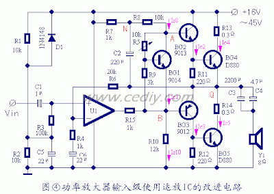
Figure 4 that is, after the improved circuit, BG1 launch junction threshold voltage and BG2, BG3, BG4 the threshold voltage with temperature change, itself, can play a role in temperature compensation. In order to reduce the output of op amp IC quiescent operating current in the output of op amp IC gifts added to the ground side of the shunt resistor R10. With the shunt resistor, the adjustment of BG2 ~ BG5 quiescent operating current can not access the first op-amp IC, directly from one of R7, R8, and R10 divider out the approximate mid-point of reference level. Start with 0 to large adjust R5 so that BG2 ~ BG5 quiescent operating current of 10mA ~ 20mA in between, and then access to op amp IC, the circuit that is able to work properly.
In addition, the output of op amp IC 1 1k current-limiting resistor in series R15, can guarantee the output op amp IC is '0 BG5 will not enter the cut-off state.
Used as a pre-op amp IC and motivate highly polar, the biggest advantage is that the output DC level input signal DC level strict consensus, a difference of not more than 0.05V. This can create OTL power amplifier consisting of two inverted output BTL power amplifier, while in the output DC level and DC level input signal are significant differences between cases, the two OTL power amplifier positive, inverting output DC level tend to be higher than 0.5V, significant effect on the work of speakers equilibrium position. BTL power amplifier positive, RP-output DC level difference between the DC level must be less than 0.1V, trumpet the work of the apparent equilibrium position will not deviate from the free position of equilibrium. Horn's work significantly deviate from the equilibrium position of the free position of equilibrium, the positive and negative direction of the mechanical vibration amplitude asymmetry, issued by the sound waves will produce distorted unnatural.
In addition, the output DC level input signal DC level strict consensus, which makes the use of positive and negative dual power supply OCL power amplifier become a reality. Otherwise, the result of the output DC level and power level of the mid-point difference between the large, will lead to a good speaker does not work properly.
As most of the op amp IC's operating voltage is not high, good performance of high-voltage op amp IC varieties of small, high prices, people can also be used with the same level pre-op amp IC differential amplifier circuit to achieve the same purpose. Figure 5 differential amplification method that is used to do most of the typical pre-circuit than shown in Figure 5 complementary symmetric OTL amplifier basic circuit characteristics of multi-purpose two identical transistors required than shown in Figure 5 improved complementary symmetric multi-purpose OTL amplifier circuits a practical transistor.
Said that they going to, not that people do not know how to design power amplifiers, but by the device of choice constraints, in different historical periods can only use the appropriate design of the circuit. In the 20th century, the late '80s, people began to more easily find properties matching using the same transistor. Due to differential amplification circuit can be extremely quiescent current and accurate design parameters for a given, do not adjust the differential amplifier tubes with a quiescent current. The circuit in Figure 5 the case of the use of 32V power, pre-differential amplifier tubes with a static current of 0.51mA ~ 0.52mA, as long as the first adjust R12 so that BG1 collector to ground terminal of the voltage dropped to 15.4V, and then adjust R5 so that BG2 ~ BG5 quiescent operating current can be between at 10mA ~ 20mA.

BG1 in adjusting the quiescent current, the same they must be adjusted to short-circuit 0 resistor R5 conditions make it BG2 ~ BG5 in a cut-off state, withhold access to the negative feedback resistor R10, with the wire will be BG6, BG0 base short-circuit.
Connected to power, adjust R12 so that the first BG1 collector to ground terminal voltage reduced 15.4V0.2V, and then adjust R5 so that BG2 ~ BG5 the quiescent operating current of 15mA. For insurance purposes, the first R8 and R9 for access into the 100Ω/2W resistors R8 and R9 on the measurement of the static voltage drop should be 1.5V. Disconnect the power supply, measuring adjustable resistor R5 and R12 in which the resistance of the actual value of their fixed resistance into the same resistance. Connected to power, R8 and R9 on the measurement of the static voltage drop should be maintained at between 1.2V ~ 1.8V. Measuring the output level should be the midpoint between the 16V0.3V. Disconnect the power, the BG6, BG0 base Qudiao between the connection wires to the negative feedback resistor R10 access to the circuit. Re-connect power, R8 and R9 on the measurement of the static voltage drop should be maintained at between 1.2V ~ 1.8V. Measuring the output level should be 16V0.2V the mid-point between the difference in charge current magnification the greater the output DC level and signal the smaller the difference between the input DC level. C1 touch with the screwdriver when the input voltage on R8 and R9 dropped significantly larger. And then replace the 0.3Ω resistors R8 and R9, connected to the horn Lyrics. When connected to the power output of the midpoint voltage of the need to rise slowly from zero, which produced only a slight impact on sound. 2 seconds later, the hands touch the C1 input Speaker will issue a "woo" the exchange of sound. The C1 input and ground (negative power supply side) short circuit, speakers should not sound, the actual will be issued by a slight background of white noise or very low voice communication hum.
Bootstrap circuit design using the power amplifier while the circuit is relatively simple, but there is lower frequency cut-off point. The introduction of the bootstrap circuit is in order to avoid when you zoom in on a half-wave there is not enough current available to complement each other to control the use, without lack of transistor used in cases, constant-current source can be used to ensure the right to zoom in on a half-wave when there is sufficient Current available to complement each other to control the use. In the meantime, the differential amplifier is also designed to provide work from the constant current source current, can greatly enhance the suppression of common-mode noise voltage ratio and relax the accuracy requirement.
Figure 6 is to use a typical constant current source power amplifier circuit, in which: BG3 and BG4 constitute a standard constant current source, the former to the front differential amplification to provide extremely 1mA constant total current, 2 only a thin charge of BG1, BG2 be 0.5mA each of the quiescent operating current; which provides a constant current of 2mA, and inspire a very BG5 quiescent operating current of 2mA equal, so that the static Q amplifier output voltage is entirely by the mid-point resistance of the same partial pressure of R13 and R14 set out, are not so large deviation from E / 2. R14 series at the bottom on the D1 is a composite pipe to compensate for the threshold voltage drop above the bottom of a single complementary than the threshold voltage drop across the tube over a PN junction voltage drop, ensuring the same from the resistance voltage divider R13 and R14 determine the midpoint voltage out of more accurate.
Stimulate the quiescent operating current is very BG5 has been on a 1V drop from the R4 and R12 resistance 200Ω identified as 2mA, also do not adjust. Therefore, in the regulation of BG7 ~ BG10 quiescent operating current when the first non-access BG4 and BG5, directly in the R13 and R14 divider out of the mid-point reference voltage and provide 0.4mA ~ 1.1mA of bias current to the BG6 working conditions, Starting from the smallest zero resistance BG7 ~ BG10 adjust R10 so that the quiescent operating current of 15 mA can be. Then replaced by a fixed resistor R10, will BG4 and BG5 access to the circuit board, amplifier immediately work properly. Although the existence of discrete element parameters, which may cause a very real incentive BG5 quiescent operating current and BG4 a small amount of difference between the current source current, differential amplification most will be the output terminal Q of the steady-state voltage deviation from the midpoint of the actual situation of automatically change the static BG1 operating current, so that the actual BG5 quiescent operating current and BG4 constant source current exactly equal. Of course, the actual quiescent operating current BG5 automatically adjusted, the differential amplification extremely quiescent operating current does not allow any one of them significantly reduced too much.
In accordance with Figure 6 in the component parameters, as long as you can make BG5 change 0.1mA quiescent operating current change 1mA, sufficient to achieve the right BG5 quiescent operating current adjustment.

However, due to constant-current source limits the incentive is a very cut-off state can provide maximum current to improve power supply voltage can not be a corresponding increase in the output amplitude. While the corresponding increase in the constant current source current can increase the output amplitude, but to inspire a very quiescent operating current will also increase accordingly, stability deteriorated.
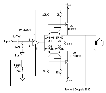
A better approach is to introduce mirror circuit, using the upper and lower symmetrical differential current-mode driver to enlarge the back of the work of complementary symmetry power amplifier tubes. Figure 7 that is used to enlarge the upper and lower symmetrical differential current-mode power amplifier to inspire a very practical circuit, due to higher output power in order to avoid overload damage to the device, circuit added to limit the maximum output current protection. Which, BG4 and BG5 constitute a mirror circuit operating current Ic5 can BG5 and BG4 operating current Ic4 remain completely equal, then the drive BG6.
Achieved by BG6, BG7 constitute the upper and lower symmetrical differential current amplification method. In this way, you can ensure that in the last half-wave signals need to stimulate greater drive current when a very, BG6 also simultaneously be able to export more to the posterior pole of the drive current power amplifier tube. To achieve the same purpose, people can also be taken in parallel and then a pair of complementary symmetrical front differential amplifier, which it has realized BG6 drive. However, the mirror circuit components requirements have not pre-high differential amplifier, using two pairs of differential pre-amplifier and the circuit can not increase any performance, no need to spend the cost of using the kind of awkward. Way to adjust the circuit shown in Figure 6 the use of the same constant current source power amplifier circuit.

From the working principle to consider, using the upper and lower symmetrical differential current amplification methods for the circuit is no longer a very encouraging defects. However, the characteristics of high-power transistors are not ideal, the output current reaches 1A above, the current magnification is only 10 ~ 25, will make driving high-power triode tube complement the work of the above must provide more than 200mA current to the posterior pole.
Complementary control its own power, often exceeding 2W, severe fever, complementary management also need to install another heat-sink. In the electronic component manufacturers have developed to produce high-power Darlington circumstances, the switch has been made within the Darlington composite pipe to make the final stage current amplification tube, we can greatly reduce complementary tube output drive current. Such as the SGS produced TIP series of high-power Darlington, in the output current to 2A above, the current magnification can reach 500 or above, which only need to complement each other with providing 20mA drive current to the posterior pole following the work of complementary tube itself power consumption to below 0.2W.
Need to modify the design parameters only based on the threshold voltage of Darlington transistor threshold voltage is equal to two ordinary times, to provide quiescent bias current shunt resistors R18, R19 doubling of resistance in order to maintain control of the quiescent operating current of complementary does not change. At the same time complementary tube BG9, BG10 base-level voltage drop between the previous increase in the threshold voltage of an ordinary transistor, its quiescent current adjustment circuit means no impact.

As Darlington is not designed for audio power amplifier developed device, the working frequency of the ceiling is not high. Limit the frequency of regular high-power transistor reached only 1MHz, developed specifically for audio power amplifiers to achieve high-power transistor can only 10MHz, preferably no more than 100MHz. Although only the audio range 10Hz ~ 20kHz, but transistor current magnification and the frequency of related, at the upper limit of operating frequency, the current magnification will drop to 1-fold.
This makes the low frequency limit of 20kHz treble amplification transistor capacity than 2kHz Alto amplification of our ability to make low, thus leading to the open-loop state, treble and tenor of the current magnification is no longer remain the same. The closed-loop negative feedback to maintain the same throughout the audio sampling magnification does not change the current mixed-signal inside pitch magnification than the tenor current situation of the low magnification, so that mixed-signal inside the treble actually higher than alto's lower magnification. Therefore, the use of high-frequency high-power transistor limit will enable mixed-signal inside Treble current magnification magnification than the tenor current decline was less.
If you are using only reached the maximum frequency of 1MHz production of high-power transistor audio power amplifier, will feel more than treble 8kHz component is seriously insufficient. Therefore, the foreign manufacturer of electronic components, has been 90 years in the 20th century developed a superior audio performance, dedicated high-power transistor amplifier. Japan 3 3 Ken Ken pipe manufactured by well-known audio power amplifier is the first dedicated high-power transistors, but they are not Darlington require superior performance of the power to do the same before the driver is a very, but also give the driver the front pole of the Power to install heat-sink.
To the 20th century, the late '80s, it developed a higher performance of high-power FET. Any high-power FET operating frequency limit can also be reached 100MHz, but at first the lack of high-voltage high-power FET, manufacturers produce more than 40W power amplifier output power or in selected high-power transistor.
In fact, making use of high-power FET amplifier than the use of high-power transistor amplifier made more convenient. But require special attention to the fact, although the effect of pipe is voltage-controlled device, but the high power FET input gate and the source exists between the large junction capacitance can be achieved around 800P, and therefore the higher the status of the operating frequency to be provided under the same charge and discharge 5mA ~ 10mA drive current.
Channeling Alliance in front of the gate resistance will affect the input junction capacitance charging and discharging, as far as possible to take a small resistance. Figure 11 that is, the practical use of high-power FET amplifier circuit, due to some high-power FET gate voltage there is no built-in limit to protect voltage regulator tube, specially in the circuit by adding a limit-voltage protection voltage regulator tube. With no built-in limit-voltage protection regulator tube high-power FET, welding wire must be used to gate and source short-circuit, welding good power FET and current-limit-voltage protection regulator tube before the gate and the source short-circuit between the wires removed. Use of high-power FET amplifier design, debug mode with the use of high-power transistor amplifier design is identical.

Should be noted that the high-power FET threshold voltage between 2V ~ 3V, (produced by Samsung, the threshold voltage of high-power FET, mostly 2V), the actual high-power FET operating voltage should not exceed the maximum allowable voltage is half the value of the maximum working peak current should not exceed the allowable current of 2 / 3 can only work to ensure safe and reliable.
This requirement is already higher than the three requirements of a wide number of machine control, machine control the actual work of the three voltage can not exceed half the value of the maximum allowable voltage, while the three-machine tube can not exceed the maximum operating current of the maximum allowable peak current of 1 / 3 before being work.
High-power FET has a great advantage is temperature-stable performance is very good, from 25 ℃ ~ 125 ℃, almost exactly the same job characteristics. Therefore, the use of high-power FET, the heat-sink can also be appropriate to allow the temperature as high as 90 ℃, while the transistors are still two of this breakdown may actually allow the temperature of the work should be limited to below 70 ℃.
4. Power Supply "High-Performance" for Power AmplifierDid not strictly control the output voltage of the midpoint value in requesting an ideal situation, power amplifier can only use a single power supply, the midpoint of the floating power supply with automatic follow ways. Just give a sufficiently large capacity storage capacitors, the actual output capability with the use of dual-power supply there is no difference between OCL output mode.
The reason for using OCL output mode, in addition to surface design a better performance can be further power amplifier, the greater practical significance is the use of positive and negative dual power supply output mode can further reduce OCL circuit background noise. In the pre-power amplifier input stage uses a differential amplifier circuit, the output DC level has been input with the signal DC level remain basically the same, a difference of less than 0.2V. In such a situation, the input signal DC level bias resistor connected to the positive and negative dual power supply potential on the midpoint, you can put a single power supply of the OTL output mode using the positive and negative dual power supply into the OCL Output way, no longer used automatically to follow the mid-point of the floating power supply.
In fact, the use of pre-op amp IC input stage can make the output DC level and signal input DC level remained nearly the same, a difference of less than 0.02V, it is precisely because the internal op amp IC also used to do a differential amplifier input stage , and generally the way of composite pipe to do the input stage differential amplifier circuit, so that flows into or out of IC positive and negative input quiescent current less than 0.1μA, the negative feedback resistor on the static DC voltage drop has been less than 0.01 V.
Identifying characteristics are always matching pipe, composite pipe can be used of course, the way to do input stage differential amplifier circuit, so that the output DC level and signal input DC level remained nearly the same, a difference of less than 0.02V, very consistent characteristic need a pair of tubes made of semiconductor materials, this is the op amp IC production process advantages. In short, the only way to change the OTL output OCL output mode, in the circuit design does not have any increase.
In fact, with work produced in class AB type power amplifier complementary symmetry there is a flaw, which is the last stage high-power amplifier tubes, static current is near the end zone, regardless of the use of high-power three tubes, or the use of high-power FET , in the end zone in the vicinity of the dynamic resistance were significantly higher than the linear dynamic resistance area should be large enough number, the actual can vary by several times to 10 times. Quiescent current is smaller, the greater the dynamic resistance. When the amplifier output voltage is zero when the speaker vibration basin will continue to be damped oscillation to stop. Voice coil moving in a magnetic field generated by currents will hinder the free vibration speaker vibration basin, if the amplifier in series with the voice coil resistance relatively large, it will cause voice coil moving in a magnetic field generated by currents decrease, reducing the role of resistance Nepal, vibration basin Vibration damping is not easy to stop down, the voice of a "dragging its feet" in divergence Shoubu Zhu situation. At the same time, the voice coil woofer speaker moving in a magnetic field induced currents produced by power amplifiers that can not be shorted out as much as possible, it would become alt prevent interference with the work unit loudspeaker drive signals. A better reason why the replay amplifier sound quality, mystery lies in the fact that it has a very low quiescent output impedance.
A power amplifier due to large, fever serious, should not be used under large operating voltage. To do this, you can use the high and low supply two sets of positive and negative manner on the final stage power amplifier tubes with current working status of implementation of the dynamic bias, so that amplifier output voltage amplitude is less than 4V when the high-power amplifier tubes with working in a current class status, the output amplitude is greater than 4V, when transformed to B status. As the rotation of working in the high-power current amplification tube is always in high-current mode of operation, the actual effect is the same way as the work of a purely A.
Figure 10 that is designed using high-power Darlington A high efficiency power amplifier typically dynamic bias circuit, in order to achieve a better dynamic offset, T1, T2 and down two high-power Darlington Complementary tube, in order to increase the threshold voltage bias circuit. Require two complementary parameters governing the same, the actual difference between the current magnification should not exceed 20%.
Dynamic bias is the result of each one and a half-wave output signal through the 4V reference value transform, require dynamic bias changing the speed limit must be more than 20KHz frequency output signal of at least 100 times higher, photoelectric conversion device isolation frequency response to be at least 1MHz, The diodes used must also be high-speed pipe. When the output signal voltage is less than 4V, the optical output transistor is cut-off state, two complementary high-power current amplification tubes were biased in the quiescent current of 1A to work, and when the output signal voltage exceeds 4V, the optical output transistor in the conduction state of two complementary high-power current amplification tube was biased at 10mA quiescent current at work. However, as the output signal voltage exceeds 4V, the current high-power amplifier tubes operating current must exceed 0.5A, 4Ω load must exceed 1A, is also equivalent to the CPI actually work. In the meantime, the output signal when the voltage is 6V or less, BG11, BG12 in the cut-off state, T3, T4 Darlington switch is also closed, T1, T2 two complementary high-power amplifier tubes with current low-voltage power supply from 8V. In the output signal voltage exceeds 6V, when, BG11, BG12 in the conduction state, T3, T4 Darlington switch also turns on, T1, T2 two complementary current amplification tubes replaced by high-power 30V high-voltage power supply, so that High-power current amplification tubes to reduce power consumption.

In the N groove and high-voltage power FET P Erdaogou easy to buy cases, can switch to high power FET to produce high-efficiency power amplifier A dynamic bias. Similarly, T1, T2 and down two high-power FET to be used complementary tube to require two complementary parameters governing the same, the actual difference between the current magnification should not exceed 20%. Bias due to the use of dynamic methods of work, bias circuit to adjust the parameters slightly more complicated.
The specific way the same way as described above, first T1, T2 from the R11, R12 series set out quiescent current regulator out of 1A, then the appropriate allocation of both the actual resistance, so that when the R12 in the short-circuit T1, T2 of the quiescent current 2mA ~ 10mA. That is not completely closed, there is no need to transfer large.

A dynamic bias in view of the main purpose of PA is to reduce the output resistance amplifier itself, in the upper and lower high-power amplifier tubes in the appropriate series current limit protection resistor, the amplifier's maximum output current limit special design in the power part of the change among the circuit.
In this way, matching power amplifier with dynamic offset the use of the CPI level of the two groups also have positive and negative power supply designed to power supply.