Search... ELectronics :

Showing posts with label Schematics. Show all posts

Constant Current Amplifier

A few days ago my friend came to the house, he shows the constant current amplifier schematics he found in http://www3.ocn.ne.jp/ ~ tima / products / ccamp / ccamp.html. We discuss and discuss until a few days. My friend kept us curious and eager to assemble.

Schematic Constant Current Amplifier Original
Schematic Constant Current Amplifier Modified


Modified schematic


I've assembled Constant Current Amplifier, but I do not really remember very well, probably from DIY Nelson Pass Zen. Constant Current Amplifier quite different from the single-ended Zen or its variants.

After reading and studying the sources of http://www3.ocn.ne.jp/ ~ tima / products / ccamp / ccamp.html and Hen experiment we finally managed to modify it by adding a few components.

In blind tests, the addition of these components produce a sound more amazing.

RX1 and CX1 form the LF filter. RX1 = 100 ohms and RCX1 = 1 nF. = 11 ohm RX2, RX3 = 0.22 ohm 5 Watt and CX2 = 100 nF

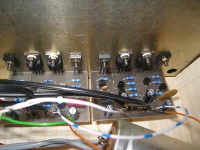
Assemble


I have a custom of using 2 Watt carbon resistor brands Phillips and my legs coated with tin WBT. I have done this long ago. I think the use of carbon 2 watt resistor produces a clear sound, more open and get a natural sound.

Therefore, I use a 2 watt resistor all unless otherwise specified.

For power supply I recommend to use A Simple Capacitance Multiplier Power Supply For Class-A Amplifiers Rod Elliott - ESP. I use a voltage source 21 Volts and 90 Volts.


Assemble survived.
(Hopefully in the next article I will discuss it in more detail)

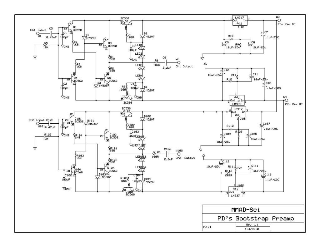
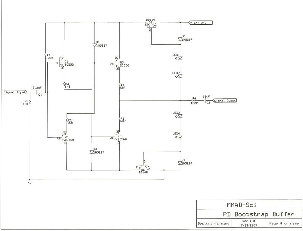
Bootstrap Buffer Based Preamp

I have been playing with a number of variations of the circuit as a free standing preamp, headphone amp, 321/729 replacements and as a potential active crossover, any and all of which may happen if there is demand. There has been strong interest in all of the threads and my bootstrap buffer preamp is up and running nicely - and for the moment it's staying. The same board should also be very handy as a headphone amp - & I'll be trying that next week.
They are different animals in so many different ways and come from completely different design philosophies. . and these are only my own observations and conclusions - so Jiim & PD feel free to chip in...please!

The starfish is definitely and very firmly in the Naim mold...and I love it for many things...lots of bass, drive and pace it really rocks..., but I can't help feeling that it's adding it's own signature to the sound. It's obviously based on maximizing the potential of the classic Naim 321 and 729 circuits and that means sorting a complex grounding scheme and multiple local regulators for power supply sensitive circuits. Accordingly it has a large and somewhat expensive BOM and is a fairly complex build.

The Bootstrap on the other hand is so much simpler and follows a minimalist design approach with as few components as possible in the signal path - it also uses symmetrical power rails and minimizes ground points in the signal path. So the BOM is smaller, the build easier and much more economical - I'll post a BOM in the next day or so. The result in the early listening is a cleaner sound with incredibly low noise and distortion, and I believe a much more truthful and honest presentation of the source material with uncanny staging and detail retrieval.

It's my expectation that I'll end up using both, the Starfish in a larger system (active Briks..) and mainly for rock & large scale orchestral music, the Boostrap in a smaller system where I'm looking for more space and precision, blues, jazz and acoustic programme material.

I guess that one of my conclusions is that just as no one system will please everyone, no one system is best for reproducing all types of material - at least not for my ears.

Schematics

 Bootstrap Buffer Based Preamp


Bootstrap Buffer Based Preamp Single Rail Supply

TURBO: A series of bipolar transistor amplifiers

25 Watt to 100 Watt, the range of TURBO is broad enough to satisfy everyone's needs.
These amplifiers are still valid and will satisfy lovers of the "bipolar" and those wishing to embark on the realization of a way "serious" quality.

In November 1980, Dominique JACOVOPOULOS published in Radio plans a series of bipolar amplifiers TURBO .

Here are excerpts:

* Amplifier TURBO 50

The amplifier TURBO 50, 50 Watt/8Ω

The article is available: http://cid-2e899d20263c980b.office.live.com/self.aspx/Public/Amplificateurs%20bipolaires%20TURBO/AMPLI%20TURBO%2050%20W%20.pdf

* Amplifier TURBO 75
 The amplifier TURBO 75, 75 Watt/8Ω


The article is available:http://cid-2e899d20263c980b.office.live.com/self.aspx/Public/Amplificateurs%20bipolaires%20TURBO/TURBO75%20v2.pdf


* Power supply

This power supply is adjustable from 30 to 40V/3A and allows to connect the two channels of a TURBO 50 and TURBO 75.

The article is available:http://cid-2e899d20263c980b.office.live.com/self.aspx/Public/ARTICLES%20DJ/ALIM%20REGULE%20L146.pdf

* Amplifier TURBO 100

Turbo 100 output power 100 Watt/8Ω

In January 1981, published in Radio Plans # 398 the 100 Turbo.

The article is available:http://cid-2e899d20263c980b.office.live.com/self.aspx/Public/Amplificateurs%20bipolaires%20TURBO/AMPLI%20BIPOLAIRE%20TURBO%20100W.pdf

* Amplifier TURBO 25

 TURBO amplifier 25 Watt/8Ω

The article is available:http://cid-2e899d20263c980b.office.live.com/self.aspx/Public/Amplificateurs%20bipolaires%20TURBO/ARTICLE%20AMPLI%20TURBO%20225%20DJ.pdf

TURBO 25 regulated power supply (polarity shown here)

Chemical charge a capacitor to smooth voltage at 100 Hz has too much work to undergo more random shocks for a long time. Its longevity depends greatly on operating conditions, performance related to them.
TURBO in the diet, the filter head C 1 assumes the thankless role.

But the sound is extracted from C6 is charged at constant voltage by the voltage stabilizer interposed between these two chemicals. Here we have a system with rapid transfer of energy under the control of the valve that is the electronic ballast transistor. This ensures the best performance in chemical output that does not suffer as current variations.


Extract from Article TURBO 25

Plans Radio 403, 06/1981

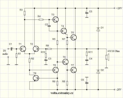
50 watts transistor amplifier

The amplifier and speakers that can handle medium-power is designed to provide a strictly amateur. Accidental overloads can damage the speakers, it is not appropriate for small systems.

What amp settings do not contain an element of the first connection wiring must be careful to work with.
Characteristics of the transistor, the fan or heat sink is cooled enough to find out if you need to focus!

Tech. parameters:
Power: + - 28V
Power: 50W / 4 ohms
Input sensitivity: 250mW of
Input resistance: 50 kOhm
Frequency range: 30Hz to - 30kHz

Optimal mobile recording portable player to another amplifier Multi Media.


Here, the schematics this power amplifier


List of components:
R1, R2, R9 - 56K
R3 - 3K3
R4, R6 - 100R
R5 - 220R
R7, R8 - 120R
R10 - 1K
R11 - 1R
C1 - in 1μF / 35V
C2 - 33P - Ceramics
C3 - the 100μF/35V
C4 - 100 N (220N) - Ceramic
C5, C6 - 4.7 UF / 35V
D1, D2 - 1N4007
T1, T2, T9 - BC546
Q3 - BC640
T4 - BD139
T5, T7 - BD711
T6 - BD140
T8 - BC639

Following the DC voltage amplifier and limiter speaker protection is needed.


source: http://www.volta.estranky.cz/clanky/zesilovace-a-predzesilovace/tranzistorovy_zesilovac_50_W.2.html

100 Watt Audio Power Amplifier

This is an exceptionally well designed amplifier, with a lot of power reserve, high fidelity, low distortion, good S/N ratio, high sensitivity, low consumption and full protection. Having all these almost ideal characteristics this amplifier is likely to become the basic building block of your future high fidelity system, or it can also become the element that will upgrade your existing system.

How it Works

The circuit works from a symmetrical ñ 40 VDC power supply and draws a maximum current of 2.6 A. The input circuit of the amplifier is a differential amplifier built around Q4 and Q5 that employ DC feedback thus preventing any DC voltage from appearing across the speaker with the usual destructive results. Q11 acts as a current source and ensures that the input stage draws a constant current of 1 mA.

The signal which appears as a voltage drop across the resistor connected in series with the collector of Q4 is used to drive the DARLINGTON pair Q3, Q2 which together with the constant current source of 7 mA that is Q10, form the driver stage. This stage operates in class A and is driving the complementary output stage Q1, Q9. The transistor Q7 is used to balance the circuit at different temperatures and must be mounted on the heatsink between the out put transistors. The feedback loop which consists of R8, R9, C2, C3 provides AC stability to the circuit. The circuit also incorporates a protection stage that makes it virtually indestructible. This protection circuit is built around Q6, Q8. If for whatever reason the output remains connected on one supply rail and the common the output is also protected from high DC voltages that could burn the speakers. The supply rails should be protected by 2 A fuses for the 8 ohm version and 3 A for the 4 ohm.


Technical Specifications - Characteristics

Output power (f=1 KHz, d=0.5 %): 100 W in 8 ohm
Supply voltage: ................  40 V
Quiescent current: ............. 50 mA
Maximum current: ............... 2.6 A
Sensitivity: . 600 mV
Frequency response: ............ 10-35000 Hz (-1 dB)
Distortion HD: ................. 0.01 %
Intermodulation dist.: ......... 0.02 %
Signal/noise: 83 dBConstruction

PLEASE READ THIS BEFORE YOU START CONSTRUCTION

To cater for those who wish to use 4 ohm speakers with this amplifier the Kit includes the necessary components for both versions. The components that differ are R3,4,17 and 23. If you build the 8 ohm version then you must also include in the circuit R28 and D7, D8 which are not used in the 4 ohm version. As you see all the components are already marked on the component side of the p.c. board.

The construction is made this way much simpler. Start the construction from the pins and the jumper connections, continue with the resistors and the capacitors and last solder in place the semiconductors. Check each resistor before soldering it, to see if its colours match those in the component list. Be careful with the electrolytic capacitors because their polarity should be respected. The polarity of those capacitors is marked on their bodies and on the component side of the p.c. board.

NOTE: On the p.c. board next to R2, R16 are marked two other resistors which do not appear in the circuit diagram but are included in the components. They are of 1 ohm 2 W (brown, black, gold) and must be included in the circuit. Take care when you are soldering the semiconductors because if you overheat them they can be damaged.

The output transistors should be mounted on the heatsink that is included in the kit. Take care not to short circuit them with the heatsink and we recommend that you use some HTC between the transistor body and the sink in order to improve heat dissipation. Follow the diagram for the mounting of the power transistors as it shows clearly how to insert the insulators and the screws. Q7 should be made to touch the heatsink and is a good idea to use a bit of HTC between its casing and the surface of the heatsink.

When you finish the construction of your project clean the board thoroughly with a solvent to remove all flux residues and make a careful visual inspection to make sure there are no mistakes, components missing and short circuits across adjacent tracks on the board. If everything is OK you can make the following connections: Input: 3 (signal), 5 (common) Output: 7 (signal), 6 (common) Supply: 1 (-40 VDC), 2 (+40 VDC) 5 (0 VDC)

Connect a milliammeter in series with the power supply, short the input of the amplifier, turn the power ON and adjust the trimmer P1 so that the quiescent current is about 50 mA. When you finish this adjustment remove the shunt from the input and connect the output of a preamplifier to it. Connect the pre amplifier to a suitable source and turn everything ON.

The signal should be heard from the speakers clear and undistorted. First of all let us consider a few basics in building electronic circuits on a printed circuit board. The board is made of a thin insulating

material clad with a thin layer of conductive copper that is shaped in such a way as to form the necessary conductors between the various components of the circuit. The use of a properly designed printed circuit board is very desirable as it speeds construction up considerably and reduces the possibility of making errors. Smart Kit boards also come pre-drilled and with the outline of the components and their identification printed on the component side to make construction easier. To protect the board during storage from oxidation and assure it gets to you in perfect condition the copper is tinned during manufacturing and covered with a special varnish that protects it from getting oxidised and makes soldering easier. Soldering the components to the board is the only way to build your circuit and from the way you do it depends greatly your success or failure. This work is not very difficult and if you stick to a few rules you should have no problems. The soldering iron that you use must be light and its power should not exceed the 25 Watts. The tip should be fine and must be kept clean at all times. For this purpose come very handy specially made sponges that are kept wet and from time to time you can wipe the hot tip on them to remove all the residues that tend to accumulate on it.
 DO NOT file or sandpaper a dirty or worn out tip. If the tip cannot be cleaned, replace it. There are many different types of solder in the market and you should choose a good quality one that contains the necessary flux in its core, to assure a perfect joint every time.
DO NOT use soldering flux apart from that which is already included in your solder. Too much flux can cause many problems and is one of the main causes of circuit malfunction. If nevertheless you have to use extra flux, as it is the case when you have to tin copper wires, clean it very thoroughly after you finish your work. In order to solder a component correctly you should do the following:

  • Clean the component leads with a small piece of emery paper. - Bend them at the correct distance from the component body and insert the component in its place on the board.

  • You may find sometimes a component with heavier gauge leads than usual, that are too thick to enter in the holes of the p.c. board. In this case use a mini drill to enlarge the holes slightly. Do not make the holes too large as this is going to make soldering difficult afterwards.

  • Take the hot iron and place its tip on the component lead while holding the end of the solder wire at the point where the lead emerges from the board. The iron tip must touch the lead slightly above the p.c. board.

  • When the solder starts to melt and flow, wait till it covers evenly the area around the hole and the flux boils and gets out from underneath the solder. The whole operation should not take more than 5 seconds. Remove the iron and leave the solder to cool naturally without blowing on it or moving the component. If everything was done properly the surface of the joint must have a bright metallic finish and its edges should be smoothly ended on the component lead and the board track. If the solder looks dull, cracked, or has the shape of a blob then you have made a dry joint and you should remove the solder (with a pump, or a solder wick) and redo it.

  • Take care not to overheat the tracks as it is very easy to lift them from the board and break them.

  • When you are soldering a sensitive component it is good practice to hold the lead from the component side of the board with a pair of long-nose pliers to divert any heat that could possibly damage the component.

  • Make sure that you do not use more solder than it is necessary as you are running the risk of short-circuiting adjacent tracks on the board, especially if they are very close together.

  • When you finish your work cut off the excess of the component leads and clean the board thoroughly with a suitable solvent to remove all flux residues that still remain on it.
If it does not work

Check your work for possible dry joints, bridges across adjacent tracks or soldering flux residues that usually cause problems. Check again all the external connections to and from the circuit to see if there is a mistake there.


  • See that there are no components missing or inserted in the wrong places.

  • Make sure that all the polarised components have been soldered the right way round. - Make sure the supply has the correct voltage and is connected the right way round to your circuit.

  • Check your project for faulty or damaged components. If everything checks and your project still fails to work, please contact your retailer and the Smart Kit Service will repair it for you.


L1 : 10 turns with wire 0,5mm turned on a restistor of 1W

If you use a 4Ohm speaker you will place R3,4,17,23 at the board.

If you use a 8Ohm speaker you will place D7 D8 and R28.

For R2 and R16 if you don't find a 0,47Ohm place two of 1 Ohm parallel.

R16 must be 0,47Ohm...the 1Ohm must be a typographical error, take care of this, i haven't tested it.

Compact High-Performance 12V 20W Stereo Amplifier

Amplifiers which run from 12V DC generally don’t put out much power and they are usually not hifi as well. But this little stereo amplifier ticks the power and low distortion boxes. With a 14.4V supply, it will deliver 20 watts per channel into 4-ohm loads at clipping while harmonic distortion at lower power levels is typically less than 0.03%.

This is an ideal project for anyone wanting a compact stereo amplifier that can run from a 12V battery. It could be just the ticket for buskers who want a small but gutsy amplifier which will run from an SLA battery or it could used anywhere that 12V DC is available – in cars, recreational vehicles, remote houses with 12V DC power or where ever.

12 Volt 20W Stereo Amplifier circuit schematic

Because it runs from DC, it will be an ideal beginner’s or schoolie’s project, with no 240VAC power supply to worry about. You can run it from a 12V battery or a DC plugpack. But while it may be compact and simple to build, there is no need to apologise for “just average” performance. In listening tests from a range of compact discs, we were very impressed with the sound quality.

Long-time readers might recall that we presented a similar 12V power amplifier design back in May 2001. It was a similar configuration to this one but it is now completely over-shadowed by the much lower distortion and greatly improved signal-to-noise ratio of this new design. In fact, let’s be honest: the previous unit is not a patch on this new design. It used two TDA1519A ICs which resulted in distortion figures above 1% virtually across the board and a signal-to-noise ratio of only -69dB unweighted.

20W Stereo Amplifier circuit schematic

However, by using the TDA­7377 power amplifier IC and making some other improvements, the THD (total harmonic distortion) of the new design is about 50 times better than the older unit (see performance graphs for details). The bottom line is that the THD under typical conditions is around just 0.03% or less. It is also able to deliver more output power due to the improved output transistors in the new power amplifier IC.

In addition, its idle power consumption is low – not much more than 1W. As a result, if you don’t push it too hard it will run cool and won’t drain the battery too quickly. And because the IC has self-protection circuitry, it’s just about indestructible. It will self-limit or shut down if it overheats and the outputs are deactivated if they are shorted.

Circuit diagram:
12V 20W Stereo Amplifier circuit schematic

With a 12V supply, the largest voltage swing a conventional solid-state power amplifier can generate is ±6V. This results in a meagre 4.5W RMS into 4O and 2.25W RMS into 8O, without considering losses in the output transistors. Even if the DC supply is around 14.4V (the maximum that can normally be expected from a 12V car battery), that only brings the power figures up to 6.48W and 3.24W for 4O and 8O loads respectively – still not really enough.

There are three common solutions to this problem. The first is to boost the supply voltage using a switchmode DC converter. This greatly increases the cost and complexity of the amplifier but it is one way of getting a lot of power from a 12V supply. However, we wanted to keep this project simple and that rules out this technique.

Parts layout:
PCB layout of compact 12V 20W Stereo Amplifier circuit schematic

There are variations on the boosting method, such as the class H architecture used in the TDA1562Q IC featured in the Portapal PA Amplifier (SILICON CHIP, February 2003). It is able to achieve 40W/channel but with >0.1% THD. In that case, the amplifier output itself provides the switching for a charge pump. The second method is to lower the speaker impedance. Some car speakers have an impedance as low as 2O, which allows twice as much power to be delivered at the same supply voltage. However, we don’t want to restrict this amplifier to 2O loudspeakers.
Author: Nicholas Vinen - Copyright: Silicon Chip

Stereo Audio Power Amplifier 11 Watt using LM4752

Featuring drives 4 Ohm and 8 Ohm loads, single supply operation, compact 7-lead TO-220 package, wide supply range 9V – 40V, internal thermal protection, internal gain resistors (AV = 34 dB), the LM4752 is a stereo audio application circuit of Stereo Audio Power Amplifier 11Watt using LM4752. amplifier capable of delivering 11 Watt per channel of continuous average output power to a 4 Ohm load, or 7 Watt per channel into 8 Ohm using a single 24V supply at 10% THD+N. This stereo audio amplifier is applied mostly in multimedia speakers, stereo TVs, Mini component stereos, and compact stereos.

schemtic digram circuit of Stereo Audio Power Amplifier 11 Watt using LM4752


The following article (well actually datasheet) contains detail information about LM4752 Stereo Audio Power Amplifier 11 Watt description, illustration, schematics and circuit diagrams, specification, key features, application, connection diagrams, absolute maximum ratings, operating ratings, electrical characteristics, test circuit, equivalent schematic diagram, system application circuit, external components description, typical performance characteristics and physical dimension. Here is a quotation from the LM4752 datasheet:

“Proper PC board layout is essential for good circuit performance. When laying out a PC board for an audio power amplifier, particular attention must be paid to the routing of the output signal ground returns relative to the input signal and bias capacitor grounds. To prevent any ground loops, the ground returns for the output signals should be routed separately and brought together at the supply ground.”

Find more about Stereo Audio Power Amplifier 11 Watt using LM4752 here – 22 pages of PDF filetype. (source: national.com). Find also other Audio Amplifier application you might be looking for.

External link:

LM4752 Stereo Audio Power Amplifier 11 Watt Datasheet – www.national.com

author: Wiring Diagram
e-mail:
web site: http://www.wiringdiagrams21.com/

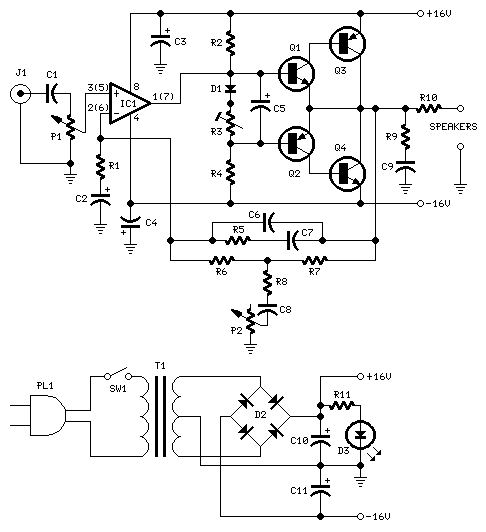
10 Watt Audio Power Amplifier with Bass-boost

Parts:
P1 22K Log.Potentiometer (Dual-gang for stereo)
P2 100K Log.Potentiometer (Dual-gang for stereo)
R1 820R 1/4W Resistor
R2,R4,R8 4K7 1/4W Resistors
R3 500R 1/2W Trimmer Cermet
R5 82K 1/4W Resistor
R6,R7 47K 1/4W Resistors
R9 10R 1/2W Resistor
R10 R22 4W Resistor (wirewound)
C1,C8 470nF 63V Polyester Capacitor
C2,C5 100uF 25V Electrolytic Capacitors
C3,C4 470uF 25V Electrolytic Capacitors
C6 47pF 63V Ceramic or Polystyrene Capacitor
C7 10nF 63V Polyester Capacitor
C9 100nF 63V Polyester Capacitor
D1 1N4148 75V 150mA Diode
IC1 NE5532 Low noise Dual Op-amp
Q1 BC547B 45V 100mA NPN Transistor
Q2 BC557B 45V 100mA PNP Transistor
Q3 TIP42A 60V 6A PNP Transistor
Q4 TIP41A 60V 6A NPN Transistor
J1 RCA audio input socket

Power supply parts:
R11 1K5 1/4W Resistor
C10,C11 4700uF 25V Electrolytic Capacitors
D2 100V 4A Diode bridge
D3 5mm. Red LED
T1 220V Primary, 12 + 12V Secondary 24-30VA Mains transformer
PL1 Male Mains plug
SW1 SPST Mains switch

schematic/circuit diagram

schematic diagram circuit of 10 Watt Audio Power Amplifier with Bass-boost

 Comments:
This design is based on the 18 Watt Audio Amplifier, and was developed mainly to satisfy the requests of correspondents unable to locate the TLE2141C chip. It uses the widespread NE5532 or TL072 for Excellent sound use ic OPA2134 Dual IC but, obviously, its power output will be comprised in the 9.5 - 11.5W range, as the supply rails cannot exceed ±18V.

As amplifiers of this kind are frequently used to drive small loudspeaker cabinets, the bass frequency range is rather sacrificed. Therefore a bass-boost control was inserted in the feedback loop of the amplifier, in order to overcome this problem without quality losses. The bass lift curve can reach a maximum of +16.4dB @ 50Hz. In any case, even when the bass control is rotated fully counterclockwise, the amplifier frequency response shows a gentle raising curve: +0.8dB @ 400Hz, +4.7dB @ 100Hz and +6dB @ 50Hz (referred to 1KHz).

Notes:
Can be directly connected to CD players, tuners and tape recorders.
Schematic shows left channel only, but C3, C4, IC1 and the power supply are common to both channels.
Numbers in parentheses show IC1 right channel pin connections.
A log type for P2 ensures a more linear regulation of bass-boost.
Don't exceed 18 + 18V supply.
Q3 and Q4 must be mounted on heatsink.
D1 must be in thermal contact with Q1.
Quiescent current (best measured with an Avo-meter in series with Q3 Emitter) is not critical.
Set the volume control to the minimum and R3 to its minimum resistance.
Power-on the circuit and adjust R3 to read a current drawing of about 20 to 25mA.
Wait about 15 minutes, watch if the current is varying and readjust if necessary.
A correct grounding is very important to eliminate hum and ground loops. Connect in the same point the ground sides of J1, P1, C2, C3 &C4. Connect C9 at the output ground.
Then connect separately the input and output grounds at the power supply ground.

Technical data:
Output power: 10 Watt RMS @ 8 Ohm (1KHz sinewave)
Sensitivity: 115 to 180mV input for 10W output (depending on P2 control position)
Frequency response: See Comments above
Total harmonic distortion @ 1KHz: 0.1W 0.009% 1W 0.004% 10W 0.005%
Total harmonic distortion @ 100Hz: 0.1W 0.009% 1W 0.007% 10W 0.012%
Total harmonic distortion @10KHz: 0.1W 0.056% 1W 0.01% 10W 0.018%
Total harmonic distortion @ 100Hz and full boost: 1W 0.015% 10W 0.03%
Max. bass-boost referred to 1KHz: 400Hz = +5dB; 200Hz = +7.3dB; 100Hz = +12dB; 50Hz = +16.4dB; 30Hz = +13.3dB
Unconditionally stable on capacitive loads

author: RED Free Circuit Designs
e-mail:
web site: http://www.redcircuits.com/

TDA1566 Car Audio Power Amplifier

The TDA1566 is a car audio power amplifier with a complementary output stage realized in BCDMOS. The TDA1566 has two Bridge Tied Load (BTL) output stages.
The TDA1566 can be configured in a single BTL mode and drive a 1 Ω load. For the single BTL mode it is necessary to connect on the Printed-Circuit Board (PCB) the outputs of both BTL channels in parallel.

The TDA1566 is a car audio power amplifier, whose schemematic is shown below,  built on a model schemematic include chips TDA1566. The TDA1566 is a car audio power amplifier does not require the establishment and therefore suitable for repetition, even beginners.
In a unipolar power load (speaker system) includes a bridge circuit which does not  require the separation of electrolytic capacitors of high capacity.


Schematic TDA1566 Car audio power amplifier


At a load resistance of 4 ohms and power voltage 14,4 Volt chip developed 2X23 Watt's, and at a load of 2 ohms - 2x40 Watt's. Tues Rejection Ratio ripple voltage 70 dB, frequency response at the level of -1 dB 20 Hz ... 20 kHz, the gain 26 dB, the level of intrinsic noise of -100 dBA.

The developed diagnostic system provides protection against overcurrent and overheating with indicator LED CLIP restrictions and protection operation LED DIAG. Mute and standby modes are included, respectively,
intermediate (from 2,5 to 4,5 V) and zero levels at the control input EN and connector STBY.

Download DataSheet clik here
skema power amplifier, high power amplifier schematic, power amplifier circuit, power amplifier schematics, power amplifier schematic, amplifier circuit diagram, rangkaian amplifier, skema amplifier, schematic diagram power amplifier, high power amplifier circuit diagram, TDA1566

50 Watts Simple Audio Power Amplifier from OSU IEEE Student Group

This simple audio power amplifier was originally designed for a circuit board workshop, conducted by the OSU IEEE Student Group. At the workshop, 20 participants each constructed this amplifier, by etching and drilling the single sided circuit board, soldering all components, and attaching a pre-built heatsink assembly with the output transistors. Three workshops were held between 1995 to 1996. Though the design is simple, these amplifers have impressive preformance, with a frequency response to approx 40 kHz, very low noise, reasonably fast slew rate, and approx 50 watts (true "RMS" power) with the proper +/- 40 volt unregulated power supply.

Someday, I'll do some substantial testing to determine exactly what the power output is, and create some more detailed pages about how to build this amplifier.


schematic

Update: the input transistor are 2N5210, not 2N2510 as shown above

board layout

part placement step 1

part placement step 2

part placement step 3

Transistor Color
2N5210 Blue
MPSA56 Pink
MPSA06 Yellow
2N3904 Green
2N3906 White

part placement step 4
These color parts placement diagrams are also available in as postscript files in a ZIP archive.

This parts list is under construction... I'm gathering part info for several lists, so pleast don't assume this list is totally correct or complete.

Qty Vendor Part # Description
1 Newark 58F508 Wakefield 421k Heatsink
2 Mouser 567-7-373-BA Low-Power TO-220 heatsink
3 Mouser 592-2N5210 Low Noise NPN, TO-92
1 Mouser 161-4215 Phono Jack, 90 deg PCB mount
1 Mouser 592-MPSA06 Medium Power NPN, TO-92
1 Mouser 592-MPSA56 Medium Power PNP, TO-92
1 Mouser 511-TIP29C Power NPN, TO-220
1 Mouser 511-TIP30C Power PNP, TO-220
1 Mouser 511-TIP33C High Power NPN, TO-218
1 Mouser 511-TIP34C High Power PNP, TO-218
2 ?? 2N3904 General Purpose NPN
1 ?? 2N3906 General Purpose PNP
2 Mouser 583-1N4742A 12V Zener Diode
5 Mouser 592-1N4148 Small Signal Diode
3 Mouser 583-1N4001 1A (slow) rectifier diode
6 Mouser 140-XLR16V100 16V 100uF Capacitor (radial)
1 Mouser 140-CD50N6-331K 330pF NPO Capacitor
1 Mouser 141-100N5-051J 51 pF NPO Capacitor
6 Mouser 140-PF2A104K 0.1uF Mylar film capacitor
2 Mouser 28PR002-0.3 3 Watt 0.3 Ohm Power resistor
1 Mouser 594-63P502 5K Top adjust cermet trim pot
2 Mouser 29SJ500-2.2K 2.2K 1/2 Watt Carbon Resistor
1/2 Injectorall PC18P 4x6 board
5

1/2 inch 4-40 machine screw
5

4-40 nut
5

4-40 lockwasher
2

Shoulder Washer
2

Insulator, TO-218 size
1

Cable Clamp
2

Red Wire, 18 AWG
1

Yellow Wire, 18 AWG
1

Orange Wire, 22 AWG
2

Blue Wire, 18 AWG
1

Purple Wire, 22 AWG
2

Green Wire, 18 AWG
1

Black Wire, 18 AWG
1

Black Wire, 22 AWG
1

White Wire, 22 AWG
1

Gray Wire, 22 AWG
1

Resistor, 4.7 Ohm, 5%
2

Resistor, 47 Ohm, 5%
6

Resistor, 220 Ohm, 5%
1

Resistor, 330 Ohm, 5%
2

Resistor, 1k, 5%
2

Resistor, 1.1k, 5%
1

Resistor, 3k, 5%
1

Resistor, 6.8k, 5%
1

Resistor, 22k, 5%
1

Resistor, 47k, 5%
1

Resistor, 10k, 1%, metal film
1

Resistor, 47k, 1%, metal film


Note: The TIP33C and TIP34C have been discontinued and are generally not available anywhere. A wide range of power transistors will work, but they should be rated for at least 100V, 8A, and 80W power dissipation. Safe area operating curves and good thermal dissipation data are rarely available, so it's a guessing game. The more expensive TO-3 package parts, such as the MJ15003 & MJ15004 will certainly be more than sufficient for replacing the TIP33C & TIP34C. The only really compelling reason to use the TIP33C & TIP34C are because they cost less and come in a TO-218 package, which requires only one mounting hole.

Wire

  Diode assembly:         Gray 22 AWG (cathode)
White 22 AWG (annode)
NPN Power Transistor: Red 18 AWG (collector)
Orange 22 AWG (base)
Yellow 18 AWG (emitter)
PNP Power Transistor: Green 18 AWG (collector)
Violet 22 AWG (base)
Blue 18 AWG (emitter)
Input Signal: No wires, PCB mount jack
Output Signal: Blue 18 AWG (from PC board)
Black 18 AWG (from power supply)
PC Board Power: Red 18 AWG (to +35V on supply)
Black 22 Awg (to ground on supply)
Green 18 AWG (to -35V on supply)

Vendors

Mouser - 800-346-6873, 619-449-2222
Newark - 800-463-9275, 503-297-1984
Injectorall - 800-878-7227, 516-563-3388

Testing

If any of these tests fail, the amp is not constructed properly... the easiest and best way to find the problem is visual inspection.
  1. Turn variable resistor fully counterclockwise (max resistance)
  2. Connect to +/- 24 volt supply with 200mA current limit. No input and no output connected. Monitor current from power supply with a current meter.
  3. Apply power... if current is above about 25 mA, shut off immediately!
  4. Measure voltage across the 1k resistor connected to the input stage and Vcc. The DC voltage should be about 2 volt, or 2 mA of current through this resistor. Eg, if Vcc is at 24 volts, the side of this resistor connected to the 2N5210 transisor ought to be at about 22 volts.
  5. Measure the DC voltage on the output line. It should be appox zero volts. -0.2 volts is probably fine.
  6. Turn the variable resistor slowly until the amplifer's current consumption is approx 50 mA. Turn slowly and be careful... if you turn too far you could damage the output transistors.
  7. Conect an oscilloscope to the output and apply a low amplitude 20 kHz square wave to the input. DO NOT connect any speakers during this test. This test should be done without the 330 pF capacitor installed. The amp should output a 20 kHz square wave with very little "ringing". It should not oscillate.
  8. Solder the 330 pF capacitor into the circuit.
  9. Shut off the power, connect audio input and a speaker. Make sure the volume is turned all the way down. Apply power... watch current meter again and shut off the power immediately if the current jumps to something much higher than 50 mA.
  10. Slowly turn up the volume and see if the amp works. DO NOT turn it up very much... the amplifier should not be operated with a supply less than +/- 30 volts. It should never be used for high volume output without a power supply rated for at least 2 amps of current (8 ohm load). After this initial test with +/- 24V at 200 mA (current limited) only a proper power supply should be used which can provide enough current.


Electronics Now

Your Ad Here
User Agreement

The creator of THIS PAGE or the ISP(s) hosting any content on this site take NO responsibility for the way you use the information provided on this site. These circuits here are for educational purposes only and SHOULD BE VIEWED ONLY. If you download any files to view them, you are agreeing to delete them within a 24 hour period. If you are affiliated with any government, or ANTI-Piracy group or any other related group or were formally a worker of one you CANNOT enter this web site, cannot access any of its files and you cannot view any of the HTML files. All the objects on this site are PRIVATE property and are meant for previewing only. If you enter this site without following these agreements you are not agreeing to these terms and you are violating code 431.322.12 of the Internet Privacy Act signed by Bill Clinton in 1995 and that means that you CANNOT threaten our ISP(s) or any person(s) or company storing these files, cannot prosecute any person(s) affiliated with this page which includes family, friends or individuals who run or enter this web site. IF YOU DO NOT AGREE TO THESE TERMS THEN LEAVE.

Disclaimer

All files are found using legitimate search engine techniques. This site does not and will not condone hacking into sites to create the links it list. We will and do assume that all links found on the search engines we use are obtained in a legal manner and the webmasters are aware of the links listed on the search engines. If you find a URL that belongs to you, and you did not realize that it was "open to the public", please use the report button to notify the blogmaster of your request to remove it. This is not an invitation for webblog haters to spam with requests to remove content they feel that is objectionable and or unacceptable. Proof of URL ownership is required.
NOTICE: This Blog Has Already Been Reviewed And Accepted By Blogger.com

© 2013. Another Electronics Circuit Schematics. Powered by Blogger.
 

blogger templates | Make Money Online