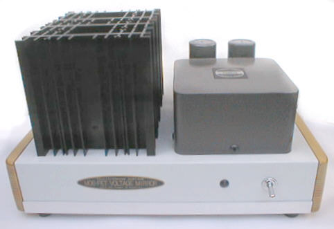
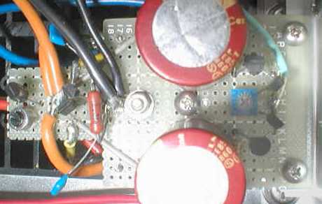
 | Lead chassis S4 (300 × 200 × 60) is used. Both sides in the handmade SHIMASHITA wood paneling. |
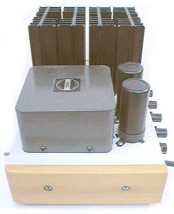 | Block on the chassis are amplified voltage capacitors and a small stage for those who for the power transformer and the radiator and looks imposing, but the real thing is compact and lightweight. |
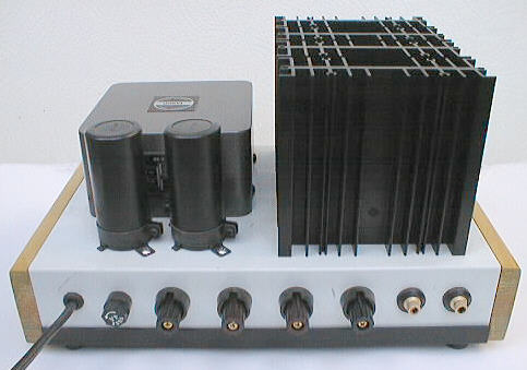 | Input terminals and output terminals to a lot of effort SUPATORON. |
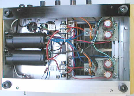 | At the bottom of the radiator board配SHI MOS-FET power output stage and to shorten the wiring, the gate入RENAKU series resistance does not even oscillation. |
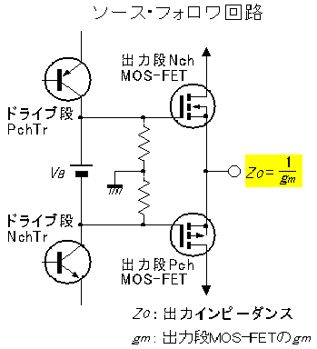
 | Just change a little wiring, the source follower circuit voltage circuits in the mirror can be changed. Miller-voltage operating conditions of the basic design is satisfactory, the source follower to change to get high-quality sound. |
Miller-voltage circuit and, as shown in Figure 1, MOS-FET source follower circuit and facing each other, the zero-bias operation to add J-FET, multiplied by the output stage to return to the local circuit.
 |
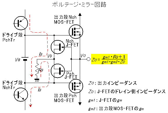 |
J-FET drain side of the drive and a collector of Tr-stage gate MOS-FET, so it is high impedance.Pch Nch of the J-FET drain and between the MOS-FET INBIDANSU low bias power are combined with V B.
Therefore, the drive signal from the current stage, I S, J-FET to the source of the flow resistance R S, J-FET source of the signal voltage V S to occur, MOS-FET to the source of power equal to V S V O voltage can be obtained.
J-FET drain side of the higher impedance Z D, the output impedance of Z O will be reduced, MOS-FET input capacity of Cis (all seen from the side of the gate capacity, and will include feedback capacity) to I see a higher frequency and lower Z D, Z O increases.
MOS-FET gate - source voltage V GS, at a maximum and not more than V B, the maximum drain current I D is limited in quantity, so the effect of preventing excessive current may have up to two out of The current limit action in the clip must be designed to SHIMAWANAI.The MOS-FET, the threshold voltage V GS (th) g m and the highest transconductance is desirable.Fortunately, switching for the rich in power MOS-FET, but the request was consistent with many.
MOS-FET used in Hitachi 2SJ113/2SK399 to.
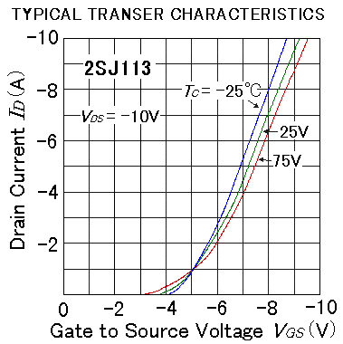
Figure 2 shows the transmission characteristics.
1A and the idling current I O and Figure 2 and V GS is the extent to 5V, V B of the V GS is about twice the 10V.
 |
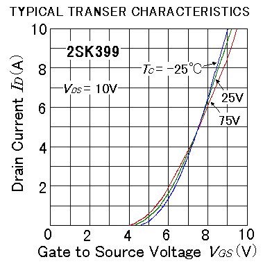 |
V GS to take a maximum of 2SJ113/2SK399 the aforementioned principles of the V B is less than 10V.
V GS in the case of a 9V about 9A So I D, 2Ω load resistance of the output voltage is also available in 18V, low enough to bear the load impedance.
For the basic design of the circuit is shown in Figure 3.
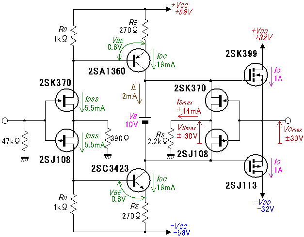
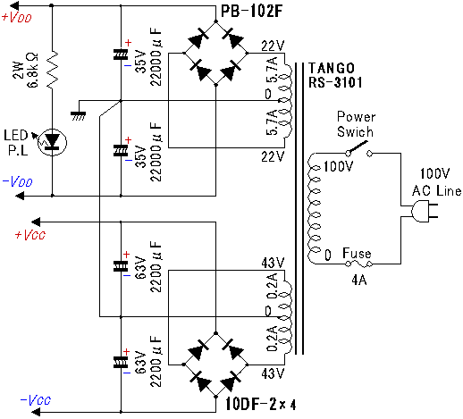
Power transformer, the tango TOROIDARUTORANSU using the RS-3101, the output stage supply voltage V DD is about 32V.
I O V B significantly higher if you set it, I D at the current clip can be larger, while the MOS-FET to increase the amount of heat, P CH channels of loss over the amount of allowable because This machine, and I O is 1A.
Table 1 from the standard table P CH = 100W (Ta = 25 ℃), T CH = 150 ℃, so Heat inside the θ i resistors θ i = (T CH - T a) / P CH = (150 ℃ - 25 ℃) / 100W = 1.25 ℃ / W. DENKA TO-3P heat sheet using the MOS-FET and the thermal resistance between the radiator, Contact thermal resistance thermal insulation resistance θ c + θ s = 0.75 ℃ / W. Below is a circuit diagram of the heat conduction. |
|
| P CH = V DD I C = 32V × 1A = 32W, so Radiator will be allowed to seek maximum temperature T f, T f = T CH - P CH (θ i +θ c +θ s =150℃ -32W×(1.25℃/W +0.75℃/W ) = 86℃ Ta ambient temperature of the radiator in the case of 50 ℃, The maximum permissible radiator heat resistance, θ f = ( T f - T a )/ P CH = ( 86℃-50℃ )/32W =1.125℃/W |
Figure 4 design radiating from the radiator to keep the temperature must be below 86 ℃.Therefore, the radiator of a flexible TF1212 (122x120 × 40) in four pieces, MOS-FET is attached by a single, open-style chassis and put on.
Bias circuit as shown in Figure 5, V B less than 1 ~ 2V zener diode voltage and low anti-adjustable instrument (VR) has been able to adjust.
[Figure 5] Bias Circuit
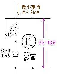
The circuit and cause a bad contact VR, I O is on the rise as a dangerous, VR is reliable in use. CRD Diode, SEMITEC Japan = E102 0.88 - 1.32 mA, 10V
The constant voltage bias circuitry to operate a minimum of about 2mA current I L.
Miller-voltage circuits used in the local feedback 2SJl08/2SK370 of the J-FET I DSS 5.5mA is ranked GR, g m and the same amount if I DSS, and other forms of J-FET is also available.
The output stage for a full swing to V S necessary, to afford to ± 30V, R S at the time that I S 2.2kΩ is in full swing is ± 14mA.When you, 2SJl08/2SK370 current flowing through the gate area covered Tr, is the gate to the low-impedance does not affect operation.
Tr stage of the drive for the operating current I S I S I SO that is half the 7mA, drive circuit and locally Biasing stage of the J-FET feedback circuitry necessary to operate because of the current sources of supply, drive stage Tr I DO idling current of theI DO > I L + I DSS + I SO I DO> I L + I DSS + I SO
= 2mA+5.5mA+7mA = 2mA +5.5 mA +7 mA
=14.5mA = 14.5mA
'91 Of the amplify circuit voltage in the February issue of its MOS-FET DARINTONANPU INBATEDDO as well as two-stage amplification of the no-return.
FET first dan level of the output stage with zero bias 2SJ108/2SK370 behavior is the same.Figure 3 is a constant,
I DO = ( R D・I DSS - V BE ) / R E I DO = (R D I DSS - V BE) / R E
=(1kΩ×5.5mA-0.6V)/0.27kΩ = (1kΩ × 5.5mA-0.6V) / 0.27kΩ
=18mA = 18mA
Thus, the above conditions are satisfied.If I DSS is a small increase in R S and will need constant change.
In addition, R S of the increase can be, if滅RASHITA Conversely, 1.8kΩ below the oscillator to the output stage.NFB also put to the Ministry of voltage amplification, or as the output stage of the oscillation Darlington to make it easier to connect.Such circuits, in order to prevent oscillation, MOS-FET and the gate necessary to insert a resistance in series there.
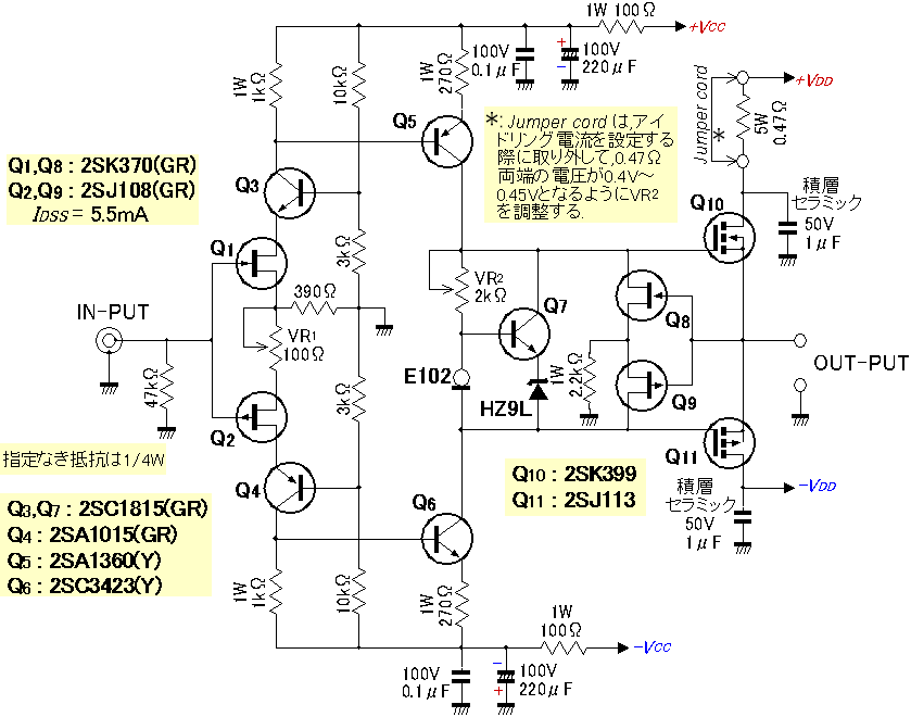
All of the library circuit is shown in Figure 6.
[Figure 6] The circuit of the machine
Amp circuit parts
Part of the power circuit
The amplification of the first dan level voltage, FET to cover the cascode-voltage connection was made.
To amplify the power of the voltage, the power to reduce noise and crosstalk, CR put filters.
To prevent oscillation, MOS-FET's drain and capacitor ground connection between the wiring to a minimum.This type of capacitor used in a significant impact on the stability of this machine 1μF use of multilayer ceramic capacitors, in a square wave output waveform was able to reduce ringing.
In making this standard to guarantee performance, Tr KONPURIMENTARIPEA and keep FET using a commercially available, and no resistance to the 5 percent level used in the selection.A pair of strict screening device, and using high-precision resistance, to get the balance of push-pull, you can further reduce distortion.
The machines used in the standard device is shown in Table 1.In addition, the unit of the standard elements of a possible substitute.
[Table 1] FET, Tr standards Maximum Ratings (Ta = 25 ℃, * Tc = 25 ℃)
Electrical Characteristics (Ta = 25 ℃)
V GDS
I G
P D
T j
I DSS
g m
C is
Electrodes connected Model name (V)
(mA)
(mW)
℃
(mA)
(mS)
(pF)
2SJ108
25
-10
200
125
-2.6~ -20
22
105
2SK370
-40
10
200
125
2.6~20
2.2
30
DGS V DSS
I D
* P CH
T CH
V GS(th)
g m
C is
(V)
(A)
(W)
℃
(V)
(S)
(pF)
2SJ113
-100
-10
100
150
-2~ -5
2
1100
2SK399
100
10
100
150
2~5
2
800
GDS V CEO
I C
P C
T j
f T
C ob
(V)
(mA)
(mW)
℃
h FE
(MHz)
(pF)
2SA1015
-50
-150
400
125
70~400
>80
4
2SC1815
50
150
400
125
70~700
>80
2
ECB V CEO
I C
P C
T j
f T
C ob
(V)
(mA)
(W)
℃
h FE
(MHz)
(pF)
2SA1360
-150
‐50
5
150
150
200
2.5
2SC3423
150
50
5
150
150
200
1.8
ECB
The production of this aircraft
A4-size chassis lead the S4 (300 × 200 × 60).
Impossible without wiring and components acrobatics on the use of the mounting, as long as stylized as a result of how the parts are in place, but not from the beginning rather than in accordance with such style, the best components and circuitry It is thought to want a place. High-current circuit in order to shorten the wiring, 22000μF blocks of storage capacitors on the inside of the chassis.
Processing of the chassis, radiator and cooling radiator for the better part of the mounting, to increase stiffness of thick reinforced with aluminum angle.
YASURI chassis in the welding marks from flat paint and Trim can be
Decoration on the front of the word processor in a black plastic sheeting was printed in gold ribbon stickers on their own.
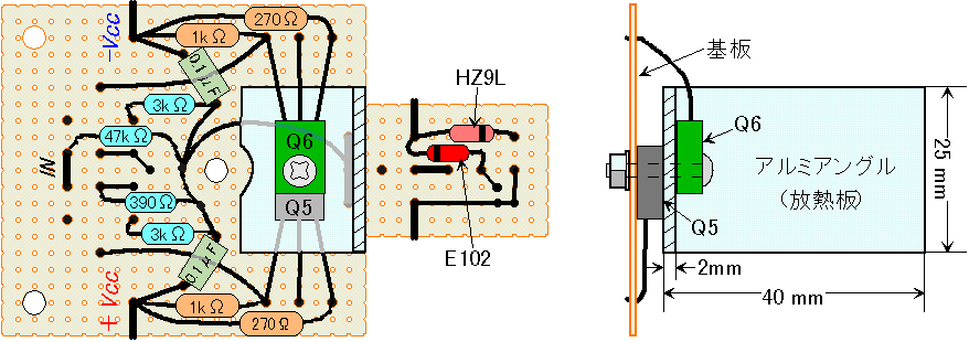
For the board, copper foil for printed circuit board wiring can not be used as a vapor.As a result of the library board, as in Figure 7, the bull's-eye of the copper foil substrate in the etching solution to remove the lead wire through a hole in the expansion of 2mm in diameter, and bring out the wiring in place of a single wire fault of 0.8mm thickness Strange.
The upper parts of the board layout | |
 | |
Place the bottom part of the board | |
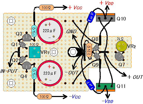 |  |
MOS-FET from the board to speed up the wiring, the board placed part of the mounting position, I sent a particular concern.
Tr two-stage during the drive, angled aluminum heat sinks are attached to the tie, the heat of the earth plate connected to the substrate, and the chassis may not have any contact.
FET complementary characteristics , so the thermal drift, it is binding, so the heat on this machine is not binding.
Upper and lower parts of the substrate is mounted on both sides, and are cross-wired to the stereo, not making a mistake when you have good circuit diagram and to see that match.
Power supply circuit, the capacitor blocks from the terminal Rch Lch and wiring into two strains, and 100Ω power supply voltage amplifier attached to the plate to lag, the output of the idling current stage of the resistance to check the terminal block 0.47Ω Mounted on.
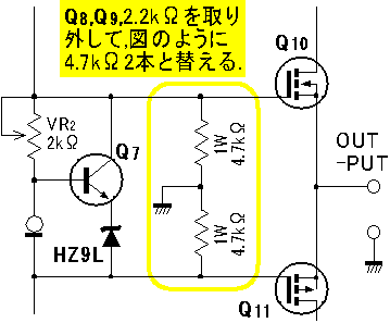
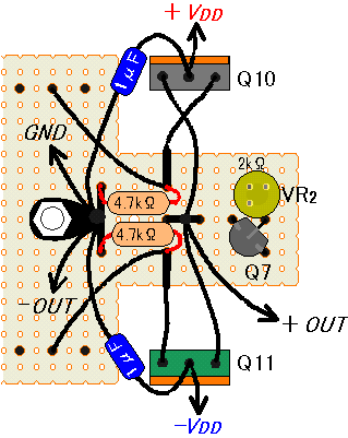
The output signal Q8, Q9 and the gate of 2.2kΩ extracted from the Earth's is a logical.Therefore, Q10, Q11 from the source of Q8, Q9 Hye-wiring of the gate, which are then wired to the output pins.But from the supply side of the Earth Hye 2.2kΩ, and the output pins and wiring.
Rectifier diode from the wiring to emit intense RIPPURUNOIZU other引KI回SHIMASU do not interfere with wiring.
MOS-FET gate of the current-carrying wires and open and the input capacity is in charge of the gate voltage to drain excessive current to flow, so beware of destruction.
Before the adjustment of the resistance VR 1 and VR 2 to leave the minimum value.
Turn the first time, in case of emergency drain and power MOS-FET 10Ω10W between the need to connect to the resistance.
Turn the output within ± 2V DC voltage, 10Ω peers verify voltage is less than 10V.
10Ω would remove the anomaly, the wiring back to normal.
The first adjustment, and idling for 1A current, VR 2 to adjust the voltage of 0.47V at both ends 0.47Ω.
If the VR 2, it is up to 0.47V If the VR 2 in the series with less than 1 ~ 2kΩ resistance in the case, contrary to 0.47V as VR 2 more than the minimum if the HZ-HZ-9L zener diode 7L exchange.
After idling 0.47Ω current settings and leave a short circuit.
DC output voltage to 0V and then to adjust the VR 1, but the power of the state暖MAっcold and heat until a stable condition change DC voltage output to 0V in any state. The machines fluctuation band around the center of the 0V.
Turn the VR 1 to increase output if the DC voltage, Q 1 source of 390Ω
After more than a measurement of adjustment, and later was able to get the property.
Changes to the source follower circuit
Lower SOSUFO If you compare the change in voltage that Miller was going to show excellence, excellence is fundamental to the circuit, the source follower of the great qualities who is also my best MASHITA.
Miller FOROWAHE voltage changes from the source, Figure 6, Figure 7, as shown in the return of local resistance to remove the FET switching can be a simple, so one can enjoy as much of the amplifier.
After the changes increase Idling a little current, so the re-adjustment is required.
In addition, changes to the circuit in the switch is no more acceptable.
The longer the oscillation circuit will be easier if the switch is running a poor contact and damage the cause of switching from the speakers.
In addition, a source follower of the voltage amplifier if you want to change the mirror, mirror voltage as the above-mentioned constraints must be met.
The characteristics of this machine
Figure 8 characteristics and the frequency of the Figure 9 crosstalk characteristics of the source and the voltage follower without a difference in the mirror, and accepted the good characteristics of the vocal cord is in the region.
RESUBONSU the high-growing region because of the high-frequency signals of the MOS-FET input current capacity can be passed through the gates - the source of signal voltage between the decrease in cost.
[Figure 8] frequency characteristics.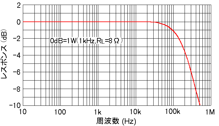
[Figure 9] characterization of crosstalk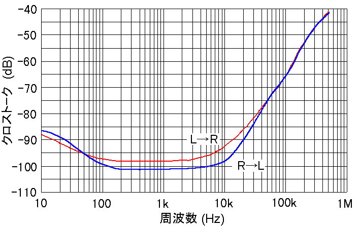
Figure 10 is characteristic of the distortion, and frequency for each individual to move parallel to the low-voltage Mirror, low-frequency effects of a localized because of the high return rate is a low distortion.
[Figure 10] distortion characteristics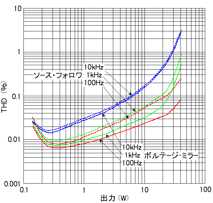
Figure 11・damping factor characteristic of the low-frequency BORUTE JIMIRA If there are more than 1,000 from 600Hz to 100kHz while much is falling in a straight line.The cause, MOS-FET input will increase capacity and frequency for the local decrease in the amount of feedback.Meanwhile, the case source follower, about 20 in the regional auditory zone is nearly constant. This is like a personality characteristics of each other's differences, which divide the sound quality is a factor.
[Figure 11] damping factor characteristics・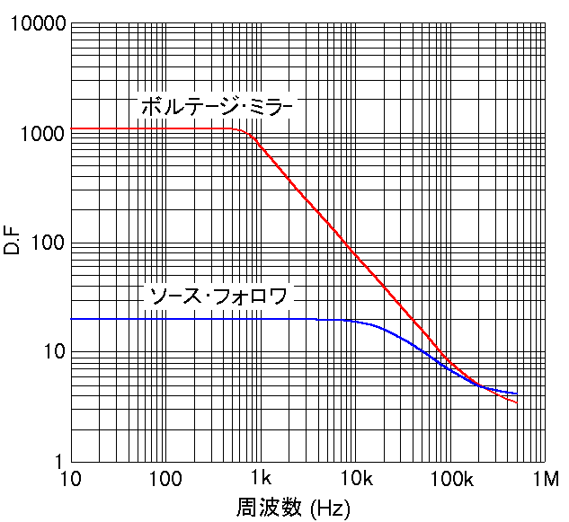
Then resist Load by 10kHz square wave output waveform of the load and capacity are shown in the photos.Enlarge to rise again to display the waveform, the ringing is legible.
| SOSU・FOROWA | Miller voltage・ |
8Ω load 4Vp-p | 8Ω load 4Vp-p |
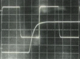 | 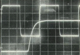 |
0.1μF load | 0.1μF load |
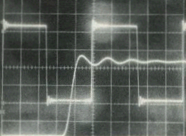 | 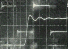 |
0.47μF load | 0.47μF load |
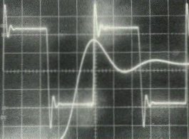 | 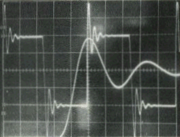 |
8Ω +0.1 μF load 4Vp-p | 8Ω load 55Vp-p |
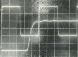 | 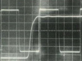 |
Miller-source voltage follower and stability in both high-capacity load is not on the oscillation.High stability and the improvement of property ambivalent relationship with, is a difficult balance.
The high-range aircraft to more than necessary that the property did not extend to higher depreciation was available taxis.
ON-OFF at the time of supply shocks 0.5Vp-p less noise and lower the residual noise Rch 140μV, Lch, and it also reduces the 130μV, and silence the cry of power transformer in the extra care.
The temperature of the radiator, but if you do not mind the location of the ventilation, can not be touched by hand and the heat is not enough.
The sound quality of the natural voltage moist Miller faction, the source follower and a faction a spectacular reduction of the thick, and to insist on individuality, both of which are difficult to discard, the悩MIMASU choice, but only if producers Can enjoy luxury.




0 comments:
Post a Comment