
from: Mike's Electric Stuff
Note - this article is original material. There is currently a plagiarised copy of it on the site of an Indian electronics magazine credited to a rip-off artist called Indrani Bose.
This page is a guide to producing consistently high quality PCBs quickly and efficiently, particularly for professional prototyping of production boards. Unlike most other PCB homebrew guides, emphasis is placed on quality, speed and repeatability rather than minimum materials cost, although the time saved by getting good PCBs every time usually saves money in the long run - even for the hobbyist, the cost of ruined PCB laminates can soon mount up!
With the methods described, you can produce repeatably good single and double-sided PCBs for through-hole and surface mount designs with track densities of 40-50 tracks per inch and 0.5mm SMD pitches.
This information has been condensed from over 20 years' experience of making PCBs, mostly as prototypes of boards to be put into production. If you follow the methods outlined here exactly, you WILL get excellent quality PCBs every time. By all means experiment, but remember that cutting corners can easily reduce quality & waste time.
I will only consider photographic methods in depth - other methods such as transfers, plotting on copper and the various 'iron-on' toner transfer systems are not really suited for fast, repeatable use. Although I've heard some good reports from some toner transfer systems, the problem with these is that the 'expensive part' is the film, and you can't really feed much less than an A5 sheet through a laser printer, so you waste a lot on small PCBs. With photoresist laminate and cheap transparency media, you only use as much of the expensive part (the board) as you need, and offcuts can usually be used later for smaller boards. Double-sided PCBs are also rather tricky with toner-transfer methods.
Artwork generation
You need to generate a positive (i.e. black = coppper) UV translucent artwork film You'll never get a good board without good artwork, so it is important to get the best possible quality at this stage.The most important thing is to get a clear sharp image with a very solid opaque black.
Nowadays, artwork will almost always be drawn using either a dedicated PCB CAD program, or a suitable drawing / graphics package. The merits of various software packages will not be discussed here, other than to say that it is absolutely essential that your PCB software prints holes in the middle of pads, to act as centre-marks when drilling. It is virtually impossible to accurately hand-drill boards without these holes. If you're looking to buy PCB software at any cost level, and want to be able to do hand-prototyping of boards before production, check that this facility is available. If you're using a general purpose CAD or graphic package, define pads as either a grouped object containing a black filled circle with a smaller concentric white filled circle on top of it, or as an unfilled circle with a thick black line style (i.e. a black ring).
When defining pad and line shapes, the following minimum sizes are recommended for reliable results: Vias (through-linking holes) : 50 mil ( 1 mil = 1/1000th of an inch, 50 mil = 0.05"), assuming 0.8mm drill size (but stick to 65 mil if you can to make drilling accuracy less critical). You can can go smaller with smaller drill sizes, but through-linking will be harder. Pads for normal components and DIL ICs : 65 mil round or square pads, with 0.8mm hole. These will allow a 12.5 mil track to pass between pins. Normal minimum line width 12.5 mil, down to 10 mil if you really need to. Centre to centre spacing of 12.5 mil tracks : 25 mil - slightly less may be possible if your printer can manage it. Take care to preserve the correct diagonal track-to-track spacing on mitred corners (pictured right, grid is 25 mil, track width 12.5 mil).
The artwork must be printed such that the printed side will be in contact with the PCB surface when UV exposing, to avoid blurred edges. In practice this means that if you design the board as seen from the component side, the bottom (solder side) layer should be printed the 'correct' way round, and the top side of a double-sided board must be printed mirrored.
Artwork quality is very dependant on both the output device and the media used, both of which will now be discussed.
Media
Contrary to what you may think, it is NOT necessary to use a transparent artwork medium - as long as it is reasonably translucent to UV, it's fine - less translucent materials may need a slightly longer exposure time. Line definition, black opaqueness and toner/ink retention are much more important. Possible print media include the following:
Clear acetate OHP transparencies - these may seem like the most obvious candidate, but are expensive, tend to crinkle or distort from laser printer heating, and toner/ink can crack off or get scratched very easily. NOT recommended.
Polyester drafting film is good but expensive, the rough surface holds ink or toner well, and it has good dimensional stability. If used in a laser printer, use the thickest stuff you can get, as the thinner film tends to crinkle too much due to the fusing heat. Even thick film can distort slightly with some laser printers. Not especially recommended, but adequate.
...and the winner is....
Tracing paper Get the thickest you can find - at least 90gsm (thinner stuff can crinkle), 120gsm is even better but harder to find. It's cheap, easily available from office or art suppliers (usually in pads the same size as normal paper sizes), has good enough UV translucency and is nearly as good as drafting film for toner retention, and stays flatter under laser-printer heat than polyester or acetate film. The stuff I use is a "Gateway Tracing", 90GSM A4 pad made by Royal Sovereign, code RS442715. Viking Direct order code Q29-RG1059
Output devices
Pen plotters - very fiddly and slow, you have to use expensive polyester drafting film (tracing paper is no good as ink flows along the fibres) and you need special inks and expensive ink pens with grooved tips to get acceptable results. Pens need frequent cleaning and clog very easily. NOT Recommended.
Ink-jet printers - Not tried them myself, but I hear very mixed reports from "perfect" to "useless"! The main problem will be getting an opaque enough black. They are so cheap that it's certainly worth a try, and with as many different media types as you can find, but don't expect the same quality you can get from lasers. It may also be worth trying an inkjet print onto paper, which can then be photocopied onto tracing paper with a good quality photocopier. I have had good reports from several people using tracing paper with HP Deskjets, but my Epson Stylus Photo750 inkjet is useless on tracing paper. Thanks to Douglas Makhija for the following info on using HP inkjets with tracing paper:
If you plot largish ground planes directly from inkjet, both 90gsm and 112gsm tracing papers crinkle slightly in these areas (the 90 more than the 112). I find that the best procedure is to allow the inkjet plot to dry thoroughly (on an HP Deskjet 670C or 895CXi set to normal - best print quality is not necessary) and then flatten out the plot under a clean sheet of paper placed under a big heavy book - I use A4 tracing paper that I get in pad form from my local artist materials shop. I find that thoroughly dried and flattened plots are perfectly re-usable.With either HP Deskjet (670C or 895CXi), I can consistently obtain 0.005 inch exposed and developed resolution.
Typesetters - for the best quality artwork, generate a Postscript or PDF file and take it to a DTP or typesetting service, and ask them to produce a positive film of it. This will usually have a resolution of at least 2400DPI, absolutely opaque black and perfect sharpness. The cost is usually 'per page' regardless of area used (UK£5 for A4 last time I did one), so if you can fit multiple copies of the PCB, or both sides onto one sheet, you'll save money. This is also a good way to do the occasional large PCB that won't fit your laser printer - sizes up to A3+ are widely available, and larger ones can also be done by more specialised services. Also a useful alternative for the highest-resolution boards that won't quite make it with other methods.
Typeset artworks are good enough for production PCBs, but most PCB houses nowadays only accept gerber data, as it's easier for them to post-process for step & repeat etc.
Laser printers - easily the best all-round solution. Very affordable, fast and good quality. The printer used must have at least 600dpi resolution for all but the simplest PCBs, as you will usually be working in multiples of 0.025" (40 tracks per inch). 300DPI does not divide into 40, 600DPI does, so you get consistent spacing and linewidth.
It is very important that the printer produces a good solid black with no toner pinholes (pinholes in larger fill areas are acceptable). If you're planning to buy a printer for PCB use, do some test prints on tracing paper to check the quality first. If the printer has a density control, set it to 'blackest'. Even the best laser printers don't generally cover large areas (e.g. ground planes) well, but this isn't usually a problem as long as fine tracks are solid. Note that the blackness of the printing on paper doesn't always mean a good opaque result on tracing paper so always check with tracing paper if you're buying a printer for PCB work.
When using tracing paper or drafting film, always use manual paper feed, and set the straightest possible paper output path, to keep the artwork as flat as possible and minimise jamming. For small PCBs, remember you can usually save paper by cutting the sheet in half (e.g. cut A4 to A5) , you may need to specify a vertical offset in your PCB software to make it print on the right part of the page.
Some laser printers have poor dimensional accuracy, which can cause problems for large PCBs, but as long as any error is linear (e.g. does not vary across the page), it can be compensated by scaling the printout in software. The only time that print accuracy is likely to be a noticeable problem is when it causes misalignment of the sides on double-sided PCBs - this can usually be avoided by careful arrangement of the plots on the page to ensure the error is the same on both layers, for example choosing whether to mirror horizontally or vertically when reversing the top-side artwork.
I use a Lexmark Optra R+ which does 1200DPI, although I only use this resolution for really fine surface mount stuff - 600DPI is usually good enough, and also feeds faster so heat distortion is reduced. When manually feeding tracing paper in this printer, you must crease the leading edge slightly downwards to avoid jamming.
Photoresist PCB laminates
Always use good quality pre-coated positive photoresist fibreglass (FR4) board. Check carefully for scratches in the protective covering, and on the surface after peeling off the covering. You don't need darkroom or subdued lighting when handling boards, as long as you avoid direct sunlight, minimuse unnecessary light exposure, and develop immediately after UV exposure.
I've always used 'Microtrak' from Mega (formerly Instagraphic) board (SS eurocard Mega order code 03-5108-1) - it develops really quickly, gives excellent resolution, and is available in thin (0.8mm) and heavy-copper flavours. It is also available from Farnell (SS eurocard order code 320-4911), but it's much cheaper direct from Mega.
I've never had any luck using spray-on photoresist, as you always get dust settling on the wet resist, and coating thickness is both critical and very hard to get even. I wouldn't recommend it unless you have access to a very clean area or drying oven, or only want to make low-resolution PCBs. Even then you probably don't really want to bother with it - life's too short to faff about coating your own laminate.
Exposure
The photoresist board needs to be exposed to ultra-violet light through the artwork, using a UV exposure box.
UV exposure units can easily be made using standard fluorescent lamp ballasts and UV tubes. For small PCBs, two or four 8 watt 12" tubes will be adequate, for larger (A3) units, four 15" 15 watt tubes are ideal. To determine the tube to glass spacing, place a sheet of tracing paper on the glass and adjust the distance to get the most even light level over the surface of the paper. Even illumination is a lot easier to obtain with 4-tube units. The UV tubes you need are those sold either as replacements for UV exposure units or insect killers. I've heard reports that 'black light' tubes for disco lighting etc. don't work very well (these have a black or dark purple appearance when off).
The tubes you want look white when off (just like normal white lamps), and light up with a light purple, which makes flourescent paper etc. glow brightly. DO NOT use short-wave UV lamps like EPROM eraser tubes or germicidal lamps, which have clear glass - these emit short-wave UV which can cause eye and skin damage, and are not suitable for PCB exposure. Mega in the UK do cheap UV bulbs as replacements for their UV boxes. RS also stock a wide range of UV tubes, including U shaped ones - search for 'insect killer' on their site. Electrical suppliers like TLC also sell UV insect-killer tubes.
A timer which switches off the UV lamps automatically is essential, and should allow exposure times from 2 to 10 minutes in 30 second increments. It is very useful if the timer has an audible indication (e.g. goes 'ping') when the timing period has completed. A mechanical or electronic timer from a scrap microwave oven would be ideal.
Dead scanners make ideal cases for homemade UV boxes, but make sure the case is deep enough - a nice old clunky one, not a modern slimline thing ( unless you don't mind using a lot of tubes to get even illumination). Although it is probably possible to make a UV box with UV LEDs, you'd need so many to get a decent exposure area that it is almost certainly not worth even thinking about unless you happen to have a few hundred of them and nothing more interesting to use them for.
Short-term eye exposure to the correct type of UV lamp is not harmful, but can cause discomfort, especially with bigger units. Use glass sheet rather than plastic for the top of the UV unit, as it will flex less and be less prone to scratches. Normal window glass works fine.
 I made up a combined unit, with switchable UV and white tubes , so it doubles as an exposure unit and a light-box for lining up double-sided artworks. If you do a lot of double-sided PCBs, it may be worth making a double-sided exposure unit, where the PCB can be sandwiched between two light sources to expose both sides simultaneously.
You will need to experiment to find the required exposure time for a particular UV unit and laminate type - expose a test piece in 30 second increments from 2 to 8 minutes, develop and use the time which gave the best image. Generally speaking, overexposure is better than underexposure. (it's easier to add the odd wire-bridge than hack off a load of unwanted copper with a Dremel or deal with lots of hairline shorts on fine-pitch tracking)
For a single-sided PCB, place the artwork, toner side up, on the UV box glass, peel off the protective film from the laminate, and place it sensitive side down on top of the artwork. The laminate must be pressed firmly down to ensure good contact all over the artwork, and this can be done either by placing weights on the back of the laminate (I use a few dead gel-cell lead-acid batteries for this), or by fitting the UV box with a hinged lid lined with foam rubber, which can be used to clamp the PCB and artwork. If you are using an old Scanner as a case, the lid will of course already be there.
To expose double-sided PCBs, print the solder side artwork as normal, and the component side mirrored. Place the two sheets together with the toner sides facing each other, and carefully line them up, checking all over the board area for correct alignment, using the holes in the pads as a guide. A light box is very handy here, but it can be done with daylight by holding the sheets on the surface of a window. If printing errors have caused slight mis-registration, align the sheets to 'avarage' the error across the whole PCB, to avoid breaking pad edges or tracks when drilling. When they are correctly aligned, staple the sheets together on two opposite sides (3 sides for big PCBs), about 10mm from the edge of the board, forming a sleeve or envelope. The gap between the board edge and staples is important to stop the paper distorting at the edge. Use the smallest stapler you can find, so the thickness of the staple is not much more than that of the PCB. Expose each side in turn, covering up the top side with a reasonably light-proof soft cover when exposing the underside - rubber mouse mats are ideal for this. Be very careful when turning the board over, to avoid the laminate slipping inside the artwork envelope and ruining the alignment.
After exposure, you can usually see a feint image of the pattern in the photosensitive layer.
Developing
The main thing to say here is DO NOT USE SODIUM HYDROXIDE for developing photoresist laminates. Use of Sodium hydroxide is the primary reason people complain about poor results when trying to photo-etch PCBs.
It is completely and utterly dreadful stuff for developing PCBs - apart from it's causticity, it's very sensitive to both temperature and concentration, and made-up solution doesn't last long. Too weak and it doesn't develop at all, too strong and it strips all the resist off. It's almost impossible to get reliable and consistent results, especially so if making PCBs in an environment with large temperature variations (garage, shed etc), as is often the case for such messy activities as PCB making. A much much better developer is a silicate based product, which comes as a liquid concentrate. I'm told this is sodium metasilicate pentahydrate Na2SiO3*5H2O (RS-Components data sheet item 690-849 and Safety data sheet). See sources below for method for making this developer.
This stuff has huge advantages over sodium hydroxide, most importantly is is very hard to over-develop. You can leave the board in for several times the normal developing time without noticeable degredation. This also means it's not temperature critical - no risk of stripping at warmer temperatures. Made-up solution also has a very long shelf-life, and lasts basically until it's worn out (and even then you can just top up with more concentrate) - the concentrate lasts essentially forever.
The lack of over-developing problems allows you to make the solution up really strong for very fast developing The recommended mix is 1 part developer to 9 parts water, but I usally make it stronger to develop MicroTrak laminate in about 5-10 seconds (yes, seconds - dip, rinse and it's done!) without the risk of over-development damage.
You can check for correct development by dipping the board in the ferric chloride very briefly (or dribbling a few drops onto the surface) - the exposed copper should turn dull pink almost instantly, leaving the track pattern sharply defined. If any shiny copper coloured areas remain, or the gaps between tracks are 'blurry', rinse and develop for a few more seconds. If the board was under-exposed, you tend to get a thin layer of resist which isn't removed by the developer. You can often remove this by gently wiping with dry paper towel (Kitchen roll, preferably non coloured/patterned!) - the dry paper towel is just abrasive enough to remove the film without damaging the resist.
You can either use a photographic developing tray or a vertical tank for developing - a tray makes it easier to see the progress of the development. You don't need a heated tray or tank unless the solution is really cold (<15°c).>
Etching
I've always used ferric chloride etchant - it's messy stuff, but easier to get and cheaper than most alternatives I've seen. It attacks ANY metal including stainless steel, so when setting up a PCB etching area, use a plastic or ceramic sink, with plastic fittings & screws wherever possible, and seal any metal screw heads etc. with silicone-rubber sealant. If copper water pipes may get splashed or dripped-on, sleeve or cover them in plastic (heat-shrink sleeving is great if you're installing new pipes). Fume extraction is not normally required, although a cover over the tank or tray when not in use is a good idea. If there is an easy way to vent fumes outside ( e.g. a cover over the tanks) this can make the fumes less objectionable but it's really not worth the hassle of setting up a powered extractor unless you have a particularly sensitive nose/throat. Power extraction is also rather problematic to do due to corrosion issues.
You should always use the hexahydrate type of ferric chloride, which is light yellow, and comes as powder or big globular granules, which should be dissolved in warm water until no more will dissolve, giving a typically muddy brown solution. Adding a teaspoon of table salt helps to make the etchant clearer (looks like very very strong tea) for easier inspection.
Anhydrous ferric chloride is sometimes encountered, which is a dark green-brown crystalline powder. Avoid this stuff if at all possible Use extreme caution, as it creates a lot of heat when dissolved - always add the powder very slowly to water, do not add water to the powder, and use gloves and safety glasses You may well find that solution made from anhydrous FeCl doesn't etch at all, if so, you need to add a small amount of hydrochloric acid and leave it for a day or two. Don't add too much acid though as it will produce very corrosive and choking fumes when warmed for etching. Sorry, I don't know what constitutes ' too much' as it's many years since I used anhydrous ferric chloride.
Always take extreme care to avoid splashing when dissolving either type of FeCl - it tends to clump together in the container due to absorbing moisture, and you often get big chunks coming out of the container & splashing into the solution. It will damage eyes and permanently stain clothing and pretty much anything else - use gloves and safety glasses and wash off any skin splashes immediately.
If you're making PCBs in a professional environment, where time is money, you really should get a heated bubble-etch tank. With fresh hot ferric chloride, a PCB will etch in well under 5 minutes, compared to up to an hour without heat or agitation. Fast etching also produces better edge quality and consistent line widths.
If you aren't using a bubble tank, you need to agitate frequently to ensure even etching. Warm the etchant by putting the etching tray inside a larger tray filled with boiling water - you want the etchant to be at least 30-50ºC for sensible etch times.
Tin Plating (Don't bother...)
Update - over the last couple of years when I've been doing a much higher proportion of SMD boards, I've come to the conclusion that tin-plating is not really worth the hassle - just strip the resist, rub with wire-wool, and immediately coat with a flux pen.
Although you can get special stripping solutions and hand applicators, most resists can be dissolved off more easily and cleanly using methanol (methylated spirit). Hold the (rinsed and dried) PCB horizontal, and dribble few drops of methanol on the surface, tilting the PCB to allow it to run over the whole surface. Wait about 10 seconds, and wipe off with a paper towel dipped in methanol. Repeat if any resist remains.
For flux-coating, use a Chemtronics CW8200 flux pen. I've found that the spray-on stuff is too sticky and thick - the pen is much cleaner and easier, and also very handy for general rework use.
I've left the old section on plating below, but I don't really think it's worth it except maybe in situations where you need a finish that lasts longer than the life of a typical prototype, e.g. for edge connectors or test-point pads, or for better cosmetic appearance.
Tin-plating a PCB makes it a lot easier to solder, and is pretty much essential for surface mount boards. Unless you have access to a roller-tinning machine, chemical tinning is the only option. Unfortunately, tin-plating chemicals are expensive, but the results are usually worth it.
If you don't tin-plate the board, either leave the photoresist coating on (most resists are intended to act as soldering fluxes), or spray the board with rework flux to prevent the copper oxidising. A 'flux pen' (available from Chemtronics & Multicore) be used to coat smaller PCBs.
I use room-temperature tin plating crystals (see Sources), which produce a good finish in a few minutes. There are other tinning chemicals available, some of which require mixing with acid, or high-temperature use - I've not tried these.
Made-up tinning solution deteriorates over time, especially in contact with air, so unless you regularly make a lot of PCBs, make up small quantities at a time (just enough to cover a PCB in the tinning tray) keep the solution in a sealed bottle (ideally one of those concertina-type bottles used for some photographic solutions to exclude air), and return it to the bottle immediately after use - a few days in an open tray and it can deteriorate badly. Also take care to avoid contamination, which can very easily render the solution useless. Thoroughly rinse and dry the PCB before tinning, keep a special tray and pair of tongs specifically for tinning (to avoid contamination), and rinse them after use. Do not top-up used solution if it stops tinning - discard it, clean & rinse the tray, and make up a fresh solution.
Ensure the temperature of the tinning solution is at least 25ºC, but not more than 40ºC - if required, either put the bottle in a hot water bath, or put the tinning tray in a bigger tray filled with hot water to warm it up. Putting a PCB in cold tinning solution will usually prevent tinning, even if the temperature is subsequently raised.
Preparation is important for a good tinned finish - strip the photoresist thoroughly - although you can get special stripping solutions and hand applicators, most resists can be dissolved off more easily and cleanly using methanol (methylated spirit). Hold the (rinsed and dried) PCB horizontal, and dribble few drops of methanol on the surface, tilting the PCB to allow it to run over the whole surface. Wait about 10 seconds, and wipe off with a paper towel dipped in methanol. Repeat if any resist remains.
Rub the copper surface all over with wire wool (which gives a much better finish than abrasive paper or those rubber 'eraser blocks') until it is bright and shiny all over, wipe with a paper towel to remove the wire wool fragments, and immediately immerse the board in the tinning solution. Take care not to touch the copper surface after cleaning, as fingermarks will impair plating.
The copper should turn a silver colour within about 30 seconds, and you should leave the board for about 5 minutes, agitating occasionally (do not use bubble agitation). For double-sided PCBs, prop the PCB at an angle to ensure the solution can get to both sides.
Rinse the board thoroughly, and rub dry with paper towel to remove any tinning crystal deposits, which can spoil the finish. If the board isn't going to be soldered for a day or two, coat it with flux, either with a rework flux spray or a flux pen.
Drilling
If you're using fibreglass (FR4) board, which you almost certainly will be, you MUST use tungsten carbide drill bits - fibreglass eats normal high-speed steel (HSS) bits very rapidly, although HSS drills are OK for odd larger sizes (>2mm) that you only use occasionally where the expense of a carbide isn't justified. Carbide drill bits are expensive, and the thin ones snap very easily. When using carbide drill bits below 1mm, you MUST use a good vertical drill stand - you WILL break drill bits very quickly without one, and at UK£2-3 a pop, a drill stand will quickly pay for itself.
Carbide drill bits are available as straight-shank (i.e. the whole bit is the diameter of the hole), or thick shank (also called 'turbo' or 'reduced' shank) , where a standard size (typically about 3.5mm or 1/8") shank tapers down to the hole size. I much prefer the straight-shank type for sizes below about 1mm because they break less easily, the longer thin section providing more flexibility. Straight-shank drills are also usually cheaper, but sometimes less easy to obtain.
When drilling with carbide bits, it's important to hold the pcb down firmly, as the drill bit can snatch the board upwards as it breaks through, and this will usually break the drill bit if the board isn't held down.
Small drills for PCB use usually come with either a set of collets of various sizes or a 3-jaw chuck - sometimes the 3-jaw chuck is an optional extra, and is worth getting for the time it saves changing collets. For accuracy, however, 3-jaw chucks aren't brilliant, and small drill sizes below 1mm quickly form grooves in the jaws, preventing good grip. Below 1mm you should use collets, and buy a few extra of the smallest ones, keeping one collet per drill size, as using a larger drill in a collet will open it out so it no longer grips smaller drills well. Some cheap drills come with plastic collets - throw them away and get metal ones.
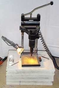 You need a good strong light on the board when drilling to ensure accuracy. I use a 12V dichroic halogen lamp (under-run at 9V to reduce brightness) mounted on a microphone gooseneck for easy positioning (shown right). It can be useful to raise the working surface about 6" above normal desk height for more comfortable viewing. Dust extraction is nice, but not essential - an occasional blow does the trick! Note that fibreglass dust & drill swarf is very abrasive and also irritating to the skin.
A foot-pedal control to switch the drill off and on is a very useful addiiton, especially when frequently changing bits.
Typical hole sizes : ICs, resistors etc. 0.8mm. Larger diodes (1N4001 etc.), square-pin headers, D connectors, IDC connectors, TO-220 leads etc. : 1.0mm, terminal blocks, trimmers etc. 1.2 to 1.5mm. Avoid hole sizes less than 0.8mm unless you really need them. Always keep at least two spare 0.8mm drill bits, as they always break just when you need a PCB really urgently. 1.0mm and larger are more resilient, but one spare is always a good idea.
When making two identical boards, it is possible to drill them both together to save time. To do this, carefully drill an 0.8mm hole in the pad nearest each corner of each of the two boards, taking care to get the centre as accurate as possible. For larger boards, drill a hole near the centre of each side as well. Lay the boards on top of each other, and insert an 0.8mm track pin (pictured below, under 'Through Plating') in 2 opposite corners, using the pins as pegs to line the PCBs up. Squeeze (with pliers or a vice ) or hammer the pins into the boards, and then insert and squeeze pins into the remaining holes. The two PCBs will now have been 'nailed' together accurately, and can be drilled together. Standard track pins are just the right length to fix standard 1.6mm PCBs together without potruding below the bottom board.
On PCBs with several hole sizes, I'd suggest drilling the larger sizes first, as this reduces the chance of accidentally under-drilling a hole - something you typically only notice when the PCB is half-assembled, making it awkward to re-drill.![]() For occasions like this, and other occasional odd sizes, I'd highly reccommend getting a micro hand-reamer This one covers sizes 1 to 5mm, made by G&J Hall (Sheffield UK), part no. GB40, available from Farnell Order code 107-232 and Rapid Electronics order code 85-0425
For occasions like this, and other occasional odd sizes, I'd highly reccommend getting a micro hand-reamer This one covers sizes 1 to 5mm, made by G&J Hall (Sheffield UK), part no. GB40, available from Farnell Order code 107-232 and Rapid Electronics order code 85-0425
For hole sizes over about 3mm, I'd recommend pilot-drilling at 1.0mm, then drilling to size with a conventional electric drill (preferably a cordless one with speed control) and standard HSS drill bit.
Cutting
 If you do any serious amount of PCB work, a small guillotine (cost about £150) is very useful, as it's by far the easiest way to cut fibreglass laminate Mega Electronics (see sources) do a very nice one. Ordinary saws (bandsaws, jigsaws, hacksaws) will be blunted quickly unless they are carbide tipped, and the dust can cause skin irritation. Although tempting if avaliable, I would particularly advise against using a bandsaw as it will not only wreck the expensive blade quickly, the inevitable fibreglass dust is likely to do long-term damage to bearings etc.
If using a hacksaw, use a long-frame type i.e. not junior) with adjsutable tension, and a medium or fine metal-cutting blade, with plenty of tension ( as tight as you can without snapping the blade). Clamp the PCB firmly, using a strip of wood to clamp the entire length of the board, close to the cut, with thin cardboard on each side of the board to avoid scratching the photoresist. Keep the saw blade angle as shallow as possible - this keeps the cut nice and straight.
A carbide tile-saw blade in a jigsaw might be worth a try, but bear in mind it's easy to accidentally scratch through the protective film when sawing, causing photoresist scratches and broken tracks on the finished board - if using a jigsaw I'd suggest adding a layer of parcel tape to increase protection .
If you have access to a sheet-metal guillotine, this is also excellent for cutting boards, providing the blade is fairly sharp.
 To make cut-outs, drill a series of small holes, punch out the blank and file to size. Alternatively use a fretsaw or small hacksaw, but be prepared to replace blades often. With practice it's possible to do corner cutouts with a guillotine but you have to be very careful not to over-cut!
A cheap nibbling tool like This one (pictured right) is very useful for making cutouts and shaping the board edge.
If you use a saw to cut the board, take care to ensure the edges are square, as burrs on the board will raise it enough from the artwork for the UV light to get between the artwork and the board Check for burrs again once you have removed the backing sheet just before exposure.
Through-plating
 When laying out double-sided boards, give some thought to how top connections will be made. Some components (e.g. resistors, unsocketed ICs) are much easier to top-solder than others (e.g. radial capacitors), so where there is a choice, make the top connection to the 'easier' component. For socketed ICs, use turned-pin sockets, preferably the type with a thick pin section under the socket body. Lift the socket slightly off the board, and solder a couple of pins on the solder side to tack it in place, and adjust so the socket is straight.. Solder all the solder side pins, then solder the required top-side pins by reheating the joint on the solder side, while applying solder to the pin and track on the component side, waiting until the solder has flowed all round the pin before removing the heat (pictured right). On dense boards, think carefully about the best order in which to insert sockets to make access to top-side pins easier. When you have finished assembling the PCB, double-check that you have top-soldered all the required top pads, as unsoldered top-side pins can cause intermittent contact and be very hard to track down.
Then when you can't get the board working, check again for top-side pins you forgot to solder - there's always at least one..!
![]() For vias (holes which link the two sides, without component pins in them), use 0.8mm snap-off linking pins (shown right), available from manyelectronics suppliers. (See Sources) These are much quicker than using pieces of wire. Just insert the bottom of the stick into the hole, bend over to snap off the bottom pin, repeat for other holes, then solder both sides. Outside the UK, they can be ordered direct from Harwin, and sample packs can be ordered from their website. Harwin part no. T1559-01, Farnell 114-3874/114-3879 (500/1000) RS 654-1276.
For vias (holes which link the two sides, without component pins in them), use 0.8mm snap-off linking pins (shown right), available from manyelectronics suppliers. (See Sources) These are much quicker than using pieces of wire. Just insert the bottom of the stick into the hole, bend over to snap off the bottom pin, repeat for other holes, then solder both sides. Outside the UK, they can be ordered direct from Harwin, and sample packs can be ordered from their website. Harwin part no. T1559-01, Farnell 114-3874/114-3879 (500/1000) RS 654-1276.
 If you need 'proper' through-plated holes, for example to connect to inaccessible top-side pins, or for underneath surface mount devices (linking pins stick out too much for use here), Multicore's "Copperset" system works well, but the kit is very expensive (£190). It uses 'bail bars' (pictured right), which consist of a rod of solder, with a copper/tin sleeve plated on the outside. The sleeve is scored at 1.6mm intervals, corresponding to the PCB thickness. The bar is inserted into the hole using a special applicator, and bent over to snap off the single bail in the hole. It is then punched with a modified automatic centre-punch, which causes the solder to splay over the ends of the plated sleeve, and also pushes the sleeve against the side of the hole. The pads are soldered each side to join the sleeve to the pads, and then the solder is removed with braid or a solder sucker to leave a clear plated hole.
 Fortunately, it is possible to use this system for plating standard 0.8mm holes without buying the full kit. You can buy the bail bars seperately as refills (£24 for 500). For the applicator, use a 0.9mm automatic pencil, (the type which has a tip like the one pictured right, e.g. Berol PCL2000), which actually works much better than the original applicator, as you get one bail for every press of the button, and it has a metal nose instead of the original plastic one. Get a small automatic centre-punch, and grind the tip off so it's completely flat - this works fine for punching the bails. For an anvil, use a thick flat piece of metal - the back of a large heatsink is perfect for this - plate all the holes before fitting any components so the bottom surface is completely flat. Holes must be drilled with a sharp 0.85mm carbide drill to get the hole size right for the plating process..
Note that if your PCB package draws pad holes the same size as the drill size, the pad hole can come out slightly larger than the drilled hole (e.g. from over-etching or non-centred drilling), causing connection problems with the plating. Ideally, the pad holes should be about 0.5mm (regardless of drill size) to make an accurate centre mark. I usually set the hole sizes to exactly half the drill size, so I know what the 'real' sizes should be when sending NC drill data for production PCBs
Update April 2007- Copperset system mentioned above appears to be out of production (possibly a victim of all this lead-free nonsense), but above section left here as replacement bail bars are still available from Farnell, order codes 463-929 and
463-942, for 0.8mm and 1.2mm respectively.
On a recent trip to Japan, I saw a similar system from Sunyahato, but I don't know of any distributors outside Japan.
Through-plating using Rivets
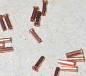
This riveting system is another way to do through-plating on dense PCBs. The rivets can be used quite easily on their own without the punch tool, just a pair of fine tweezers (and a steady hand...).
The 0.4mm rivets (pictured) fit a 0.6mm hole and so can be used on quite dense groups of 0.05" pad dia vias.
Recommended equipment
Three-tank unit comprising heated bubble etch, spray wash and developer tank. As a bare minimum, a bubble-etch tank and some way of rinsing boards. Photographic developing trays are adequate for developing and tinning.
Different sized photographic developing trays for tinning.
PCB guillotine or small sheet-metal guillotine. A Jigsaw is an alternative but you will get through baldes quickly - use medium to fine metal-cutting blades and use paper or card between the shoe-plate and the board to prevent the edge of the show damaging the resist.
PCB drill - precision drill with metal collets and good quality stand. A foot pedal on/off control is a very useful addition.
If running water is not available, get a hand-held spray bottle (as sold for garden insect sprays etc.) for rinsing PCBs.
Sources
Developer :
Thanks to Robin Moorshead for the following procedure to make silicate developer solution:
Take 200cc of "water glass", add 800cc of distilled water and stir. To this add 400g of sodium hydroxide (caustic soda).
Important safety precautions: The sodium hydroxide solid must NEVER be handled, use disposable gloves. When the sodium hydroxide dissolves in water it produces a great deal of heat so it must be added a little at a time and each portion allowed to dissolve before more is added. If the solution becomes very hot leave it to cool before adding more sodium hydroxide.
The solution is VERY caustic and it is particularly damaging to the eyes, use eye protection when making and handling it.
It also ruins clothing. Water glass is also known as "sodium silicate solution" and "egg preserver", It used in fire proofing fabrics, for waterproofing walls and making "chemical gardens". Caustic soda is used for clearing drains and available from any chemist. The solution cannot be made by dissolving solid sodium silicate.
This solution will be the same strength as the concentrate, and so will need diluting - about 1 part concentrate to 4 to 8 parts water, depending on the photoresist used and temperature.
UK
Mega Electronics, Cambridge UK 01223 893900.
Very comprehensive range of all PCB production equipment and materials at good prices. They're very helpful & friendly, take credit card orders and charge carriage at cost. They're good for obscure stuff like heavy (2 Oz /70 micron) copper and 0.8" thick laminates, unusual carbide drill sizes etc. They have their own large range of processing tanks, drills, plating lines etc. They stock the silicate based developer and tin-plating chemicals mentioned above. Unusual laminates (thin, heavy copper etc.) are sold as large sheets but they will cut them down to sensible sized panels free on request (but phone them as they sometimes miss cutting instructions in the 'comments' field on the web order form, as I found when a slightly bemused Post Office driver turned up carrying a huge sheet of 0.8mm laminate...), and they may be willing to sell smaller offcuts if you only want smaller amounts. The also do reasonably priced UV tubes as replacements for their UV boxes.
Silicate based developer - Seno 4006 (liquid concentrate, 1 litre), Mega Electronics order code 600-010
Also available in powdered form, order code 600-008 (50g, makes 1 litre), 600-007 (500g, makes 10L). I haven't tried the powdered version - the catalogue mentions a limited shelf-life of made-up solution for the powder - the liquid stuff lasts indefinitely.
PCB Guillotine 700-400 (8") 700-500 (12")
THE tool for cutting PCBs. If you do a lot of PCBs you NEED one of these.
Rapid Electronics They stock the silicate developer 34-0790 (1 litre concentrate), 34-0395 (20g powder to make 500ml), plus etchant, tanks etc. These are the Mega products, and so usually available cheaper direct from Mega.
Rapid are also incredibly cheap for a lot of run-of-the mill electronic components - much cheaper than RS, Farnell, Maplin etc.
GCL Supplier of bubble etch & processing tanks, UV exposure units and lightboxes.
![]() Snap-off linking pins for double-sided boards, and pinning PCBs for drilling 2-up : Harwin part no. T1559-01, (Farnell 143-738) (RS 435-383) I'm told they are hard to find in the US, but can be ordered direct from Harwin (boxes of 2500 for US$32.33), and sample packs (100) can be ordered free from their website by quoting the part number.
Snap-off linking pins for double-sided boards, and pinning PCBs for drilling 2-up : Harwin part no. T1559-01, (Farnell 143-738) (RS 435-383) I'm told they are hard to find in the US, but can be ordered direct from Harwin (boxes of 2500 for US$32.33), and sample packs (100) can be ordered free from their website by quoting the part number.
RS have some unusual photoresist PCB laminates from CIF to their range, including 70 micron (2 oz.) copper, 0.4 and 0.8mm mm thickness and PTFE (Duroid). They also have a reasonable range of general PCB materials, as well as a range of UV tubes (search for 'insect killer' on their site)). CPC also stock some CIF lines
Holders stock a wide range of PCB materials and equipment - although they but appear to be geared towards supplying commercial PCB houses, they tell me that they are happy to supply small users and have no minimum orders for drills, routers or FR4 laminates.
ESR stock a range of PCB equipment and materials, including some cheap reground reduced-shank carbide drill bits.
http://www.fortex.co.uk/ UK supplier of PCB making equipment
TLC (bottom of page) Sell UV tubes at very good prices
CPC (UK) sell UV tubes for exposure boxes. LP01874 (8W 12") LP01875 (15W 18"). They also do 'U' format tubes, ballasts and tube caps, as well as a range of PCB laminates etc. including some of the CIF specialist stuff like flexi.
USA
If anyone has info on good sources inside or outside the UK, please let me know & I'll add them here.
I can't be bothered with all this- where can I get small quantity PCBs made by someone..?
For prototypes, I have used PCB-Pool a lot. Quality and service has been excellent, and for 1-offs and small numbers pricing is pretty good due to lack of 1-off costs. They are rather expensive for larger numbers however.
They recently introduced a system where you can see photos of your PCBs at various stages through the production process - not sure how useful this is though..!
A number of similar pooling services have sprung up recently, but I haven't used any of them so can't comment. (any feedback welcom)
I've recently discovered a Chinese place called PCBCART - prices are excellent, and they do a lot of unusual options - thicknesses, copper weights, funky resist and silkscreen colours. I've had 5 lots of boards from them so far (Jan 07), including one batch of 4-layer PCBs, and quality/delivery have been fine. I've also had good feedback from another user who has had several thousand PCBs from them.
Payment options include Paypal or another Credit-card handling company (2co.com, who have MUCH better customer service and communications than Paypal!)
Remember to check the shipping costs when comparing prices (this only appears after you do 'add to cart'), however even with these they are really cheap for all but the smallest quantities.
At 1-5 off prototype quantities of small PCBs the one-off and shipping costs make them less competitive with places like PCB-Pool, but as soon as you get into quantities of tens & up, or even less for larger boards, they are typically very competitive.
Update 20 Mar 2007 - having had good service from PCBCART, I've had no confirmation or emails re. an order I placed recently & have heard another similar report.
Update 6 April 2007 - it seems PCBCART had some website & comms problems in March - they have since been in touch & everything appears to be back to normal.
Update 16th April 2007 - received the last lot of PCBs last week - the usual good quality (and no extra charge for 2400 holes on a 100x160mm PCB!), and I've had an order confirmation on a new PCB, so things look all OK now and I can continue to highly reccommend them. I will update this page if this situation changes - hopefully this won't be necessary.
Update 22 Aug 07 - they still seem to have occasional trouble accepting emails, in particular replies to queries that arise. I don't know if this is a genuine email problem at their end or if they just don't reply in a sensible time if they're too busy...!
My experience is that after ordering, you fairly quickly get a "processed" email, then around a day or two later get a second "confirmation" email with a delivery date. Once you get this second email, your PCBs WILL arrive on time - you get a third email with a DHL tracking number when dispatched (you need to take the spaces out of this number for it to work on the DHL site).
However if they email you with a query (e.g. to confirm panelisation details), everything goes on hold til they get your reply, and this is where the problem can arise - If I don't get a confirmation within 48 hrs I ususally fax them & things proceed OK. You need however to take this potential delay into account if you need PCBs urgently! For this reason, I don't specify a panellised PCBs unless I really need it!
Others I have not tried :
PCBTRAIN (They also offer online pricing for SM and TH component assembly).
Eurocircuits Reasonably good pricing, I have heard good reports second-hand. Ordering/payment process complicated - need to set up an account.
Olimex - I continue to hear mixed reports, especially about being difficult to deal with sometimes and not very flexible. Quality of the PCBs of theirs I've seen looks fine though.
http://www.arelectronics.co.uk/qbuild.htm Online quote calculator for SMT and conventional assembly (assy only, not PCB suppliers)
I'd welcome comments from anyone who has used either of the above.


1 comments:
Many thanks for your educational document. I am in fact at work at the moment!
pcb suppliers
,circuit board assembly
Post a Comment